Chase Fournier has a gift for making scrap look intentional. In "I Turned an Xbox One into a Flash Drive," he opens two dead Xbox One S motherboards, skips the hard drives, and goes straight for the eMMC packages. The idea is pure maker logic: extract the storage chips, reball them, mount both on one carrier, and end up with a functional USB 3.0 stick that still works years after the consoles failed.
He wanted usable recycled storage that could show old console silicon still had value. In a market where memory prices keep rising, that goal only works when the board underneath cooperates. BGA pads must survive multiple heat cycles, the controller has to see both chips cleanly, and the USB 3.0 traces need enough integrity for sequential speeds to stay usable. Everything else is just soldering.
Extracting the Chips and Getting Them to Enumerate
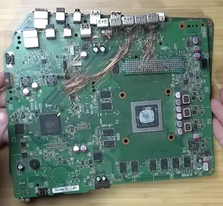
Chase starts with hot air and patience. The eMMC packages (typically Toshiba 8 GB parts that the system often reports closer to 5 GB usable) come off cleanly once temperature and flux are dialed in. After thorough cleaning, each chip goes into a programmer. Some refuse to talk until another isopropyl wipe removes the last residue. Then reballing begins: stencil, paste, reflow, and the usual cleanup when a few balls refuse to form properly.
Figure: Chip extracted from the board
Both reballed chips land on a dual-channel carrier built around the Norelsys NS1081. That controller can address up to four eMMC or SD devices and supports a RAID-0-style configuration that combines capacity. After firmware programming and initialization, the computer sees roughly 10 GB of USB 3.0 storage. CrystalDiskMark shows sequential reads near 140 MB/s and writes in the 40–64 MB/s range—solid numbers for recycled parts. Random performance is lower, but the drive is fast enough for everyday files and even storage duties on several platforms.
Figure: Reballed chips land on a dual-channel carrier built around the Norelsys NS1081
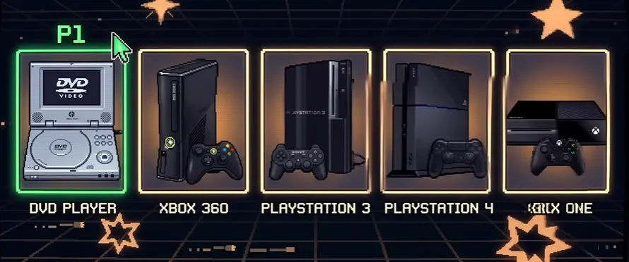
The real payoff arrives when the same stick mounts on a Raspberry Pi cyberdeck, a modded Xbox 360, a jailbroken PS3, a PS4, and finally an Xbox One itself. Watching a drive born from Xbox One silicon get recognized by an Xbox One is the circular satisfaction that keeps makers going.
What the Carrier Board Actually Needed to Deliver
The board is compact and dual-sided. The parameters that mattered most in real use:
|
Parameter |
Choice that worked |
Why it mattered |
|---|---|---|
|
Layers |
2–4 (4 preferred) |
Cleaner return paths for USB SuperSpeed and better power distribution |
|
Thickness |
1.0–1.6 mm |
Survives hot-air rework without excessive flex |
|
Copper |
1 oz outer |
Enough current capacity without undercut problems |
|
Surface finish |
ENIG |
Flat, oxidation-resistant pads essential for reliable BGA joints |
|
Impedance |
~90 Ω differential |
Keeps SuperSpeed signaling intact over short runs |
|
Via style |
Through-hole, occasionally plugged |
Solid connections under the controller and eMMC footprints |
Layout details that quietly decided success included clear pin-1 silk marks, short and length-matched differential pairs from the NS1081 to the USB connector, continuous ground under the high-speed traces, and decoupling placed tightly at both the controller and the eMMC power pins. Without those, the dual-chip setup becomes an exercise in intermittent enumeration.
The Points Where the Project Nearly Failed
The real drama unfolded during reballing. On the first reflow attempt some of the solder balls simply refused to form. Chase added more flux and ran the heat again, but the paste still would not wet properly to the pads. Rather than force a bad joint, he carefully lifted the chip off with tweezers and started over.
For the second attempt he cleaned the chip thoroughly, aligned a fresh stencil, and applied solder paste a second time to guarantee an even coating. This time the reflow succeeded and the balls formed cleanly.
Figure: First chip soldering problem and solution
To be extra safe he deliberately holding the heat source a little farther away when soldering chip 2. Even then a small amount of residual solder remained on the pads and began floating around as free-moving tin balls. Only after adding more flux and carefully coaxing the balls back into position did every joint finally stay put.
Figure: Chip 2 soldering problem and solution
That sequence—failed first reflow, tweezers removal, double paste application, successful second reflow, cautious third pass, and the floating-ball fix—is pure real-world BGA work. It also highlights why the carrier board's surface finish and pad geometry matter so much: any uneven plating or residual oxide turns exactly this kind of recovery into hours of extra labor. The fact that both eMMCs eventually seated cleanly and the NS1081 saw both channels is a direct result of surviving that messy, iterative process.
Why a Solid Prototype Board Changed the Outcome
This is the kind of project where the PCB stops being a passive part and becomes the quiet enabler. Chase's work (including the open MultiBoi multi-tool board he also shares) depends on boards that arrive with consistent ENIG finishes, accurate BGA footprints, and stack-ups that actually support the impedance the NS1081 expects. When you are hand-placing two reballed eMMCs and expecting both channels to stay reliable through heat cycles and real-world use, pad flatness and plating quality are no longer optional.
AIVON's prototype service—especially the accessible entry pricing that lets makers spin boards without hesitation—removes enough process variables that the focus can stay on the creative work. Clean solder-mask registration around fine-pitch pads, balanced copper that resists warping under hot air, and practical engineering feedback on via placement or impedance targets all reduce the chance that the board itself becomes the failure point. The result is a carrier that survives the reball-and-reflow cycle, keeps SuperSpeed signals intact enough for 140 MB/s-class sequential performance, and still fits a pocket-sized form factor.
In practice, the board did not just hold the parts. It absorbed enough of the manufacturing uncertainty that Chase could finish the project instead of fighting the fabricator.
Practical DFM Checklist for Dual-eMMC USB Carriers
|
Checkpoint |
What to specify |
Why it saves time on this exact build |
|---|---|---|
|
BGA pad finish |
ENIG |
Flat surface that accepts reballing without drama |
|
Pad geometry |
Match datasheet + modest tolerance |
Reduces opens and tombstoning |
|
SuperSpeed pair matching |
Length match under 5 mil, continuous ground |
Preserves sequential performance |
|
Decoupling |
Caps within a few millimeters of power pins |
Stable voltage under dual-chip current |
|
Thermal relief |
Balanced spokes on large pads |
Easy rework without lifting copper |
|
Silk marks |
Clear pin-1 and orientation |
Fewer assembly mistakes under magnification |
|
Mechanical |
1.6 mm / 1 oz typical |
Handles connector stress and repeated heat |
What the Finished Drive Proved
Chase started with two dead Xbox One S boards and ended with a functional 10 GB USB 3.0 drive that mounts on PCs and multiple consoles. The journey mixed pure maker enthusiasm with the practical realities of BGA rework and high-speed layout. Professional prototype support turns that kind of ambitious idea into something that enumerates reliably instead of becoming another unfinished experiment on the bench. If you have a drawer of old console boards or a dual-eMMC concept of your own, the same path is open—respect the DFM details, get a solid board in your hands, and see what the scrap still has left to give.
FAQ
Q1: Why is ENIG preferred over HASL for dual-eMMC carrier boards?
A1: ENIG delivers a flat, oxidation-resistant surface that is critical for reliable BGA reballing and reflow. HASL is too uneven for fine-pitch eMMC packages and often causes incomplete joints or alignment issues during hand assembly.
Q2: Do I really need a 4-layer stackup for a compact NS1081 USB 3.0 design?
A2: A carefully routed 2-layer board can work for very short SuperSpeed runs, but 4-layer gives continuous ground references, better power distribution, and higher confidence in 90 Ω differential impedance control—especially when two eMMC chips are drawing current simultaneously.
Q3: What BGA pad and via rules matter most for reballing success?
A3: Match pad size to the eMMC datasheet with modest tolerance, use ENIG finish, keep thermal relief balanced, and place vias so they do not create solder-starved pads. Poor pad geometry or uneven plating is the fastest way to turn a five-minute install into repeated rework.
Q4: How critical is differential pair matching on these small carriers?
A4: USB SuperSpeed pairs should stay length-matched within a few mils and ride over continuous ground. Even short runs on a dual-eMMC board will lose sequential performance if the return path is broken or the pairs are unbalanced.
Q5: What surface-finish and copper-weight combination survives repeated hot-air rework?
A5: 1 oz copper with ENIG is the practical sweet spot. It handles multiple reflow cycles without excessive undercut or warping while still providing enough current capacity for the NS1081 plus two eMMC devices.
Q6: Where should decoupling capacitors sit on an NS1081 dual-eMMC layout?
A6: Place them within a few millimeters of both the controller power pins and the eMMC VCC/VCCQ pins. Tight placement keeps voltage stable under the higher current of dual-channel operation and reduces the chance of intermittent enumeration.