 28:04
28:04
Design For Manufacturing (DFM)
Design For Manufacturing (DFM) plays a pivotal role in the electronics industry, bridging the gap between innovative PCB design and efficient production. This approach focuses on optimizing circuit board layouts and component selections to streamline manufacturing processes, reduce costs, and minimize defects. Engineers and designers who prioritize DFM early in the development cycle can avoid common pitfalls such as overly complex assemblies or material incompatibilities that lead to production delays and increased expenses. By incorporating DFM principles, professionals ensure that their designs are not only functional but also manufacturable at scale, making it an essential strategy for anyone involved in electronics prototyping or mass production. Key aspects of DFM include guidelines for component placement, trace routing, and panelization that align with fabrication capabilities. For instance, adhering to minimum spacing rules and selecting readily available parts can significantly enhance yield rates and accelerate time to market. Practical applications extend to various sectors, from consumer electronics to automotive systems, where reliability and cost-effectiveness are paramount. Best practices involve conducting DFM reviews using specialized software tools to simulate manufacturing outcomes and identify potential issues before prototypes are built. This proactive method empowers teams to iterate designs efficiently, fostering innovation while maintaining high standards of quality control. The articles tagged under Design For Manufacturing (DFM) offer in-depth explorations of these concepts, including real-world case studies and step-by-step tutorials on implementing DFM checklists. Readers can find valuable insights into emerging trends like automated DFM analysis and integration with design automation tools, helping them apply these strategies to their own projects. Diving into these resources provides the knowledge needed to refine PCB designs for optimal manufacturability.
Video Guide



Technical Articles

DFM Deep Dive: Keep Vias Away from Pads to Prevent SMT Reflow Shorts and Tantalum Capacitor Offset

The "Black Hole" on Pads: Why Via-in-Pad Must Be Filled or Avoided

DFM for D-PAK (TO-252): Prevent Solder Voids and Component Shift with Solder Mask Isolation and Segmented Pads

Deep Analysis: The BGA Rework Keep-Out Zone — Why You Must Not Place Components ≥ 3216 Directly Under a BGA

DFM in Practice: The Hidden Tolerance Trap—Why SMT Connector Locating Pins Must Be Smaller Than the Hole

PCB Hole and Slot Tolerance Conflicts: CAM Cases from Production

Manufacturing Process Study for 0.3 mm Pitch QFN Packages

Wave Soldering Fixture Design Essentials for Process Engineers

DFM in Practice: Zero-Pressure SMT Placement for Long DIMM Sockets — The Mechanics of Oval NPTH Holes and Locating Pins

How PCB CAM Resolves Blind Via Size and Edge Clearance Issues

Complete Guide to Pad Design for Through?Hole Parts in SMT (Pin-in-Paste, PIP)
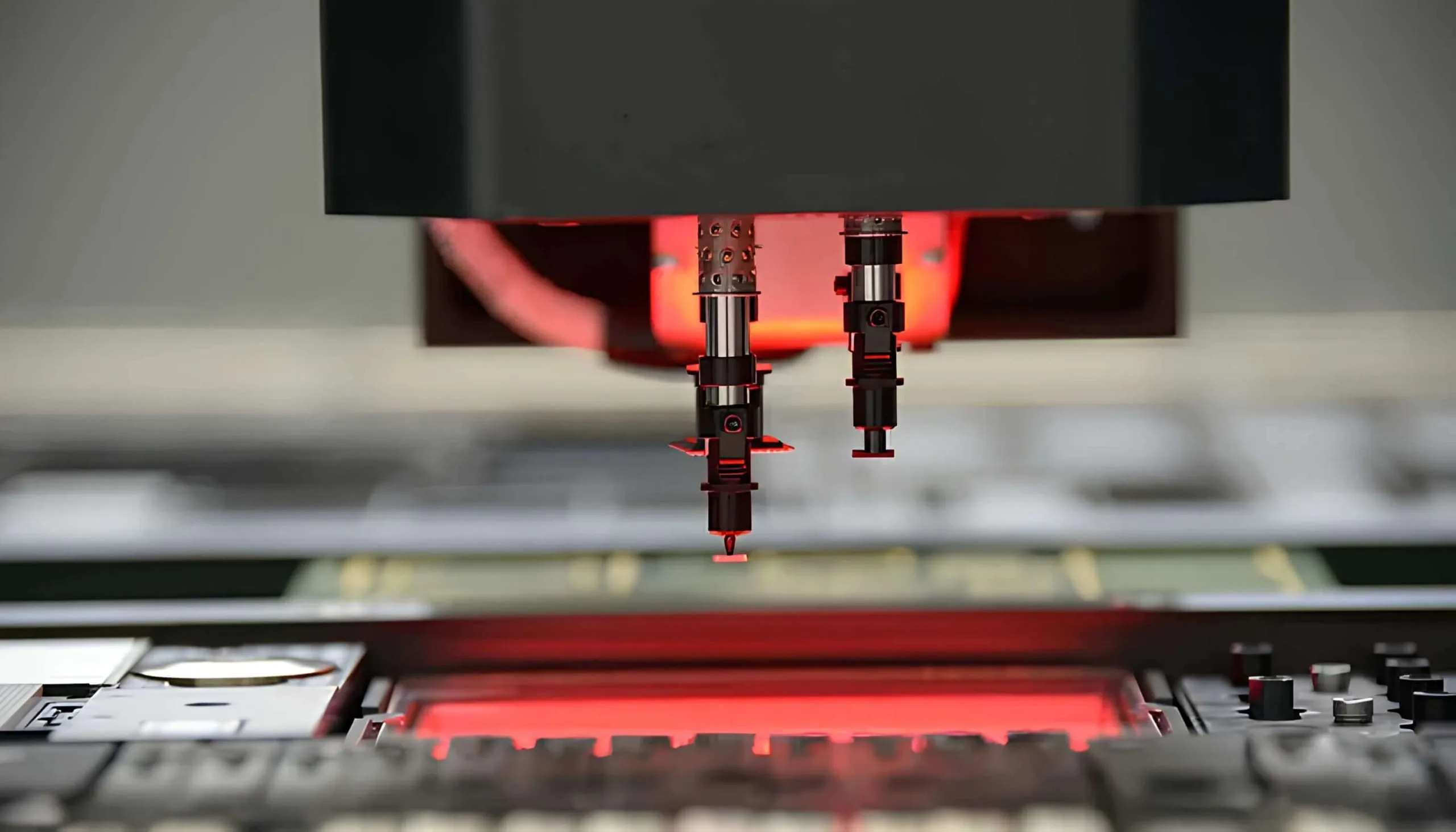
Using Cpk to Reveal the Real Accuracy of SMT Pick-and-Place Machines

DEK Stencil Printer Level/Height Calibration and Solvent Spray Mechanism Upgrade to Prevent Wiping Clogs

PCB CAM Case Study on Tight Tolerances in Backdrilling, Countersink, and Press-Fit Holes

Press-Fit PCB Hole Design Standards and Process Best Practices

Wave Soldering in Through-Hole Assembly: Practical DOE Case Studies for Yield Improvement

Why PCB CAM Must Verify PTH and NPTH Hole Definitions
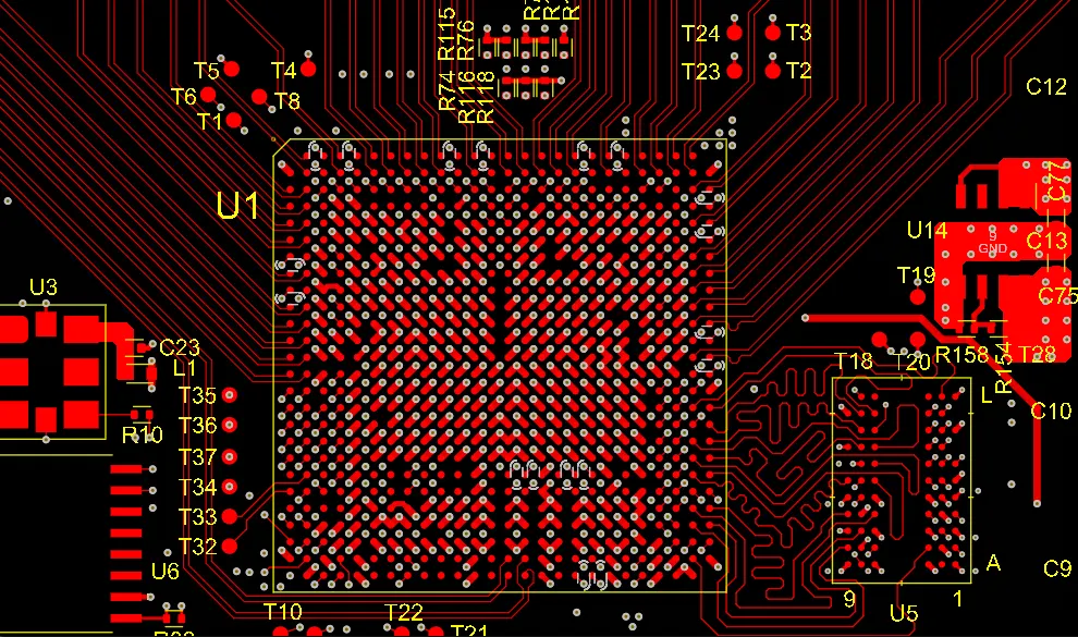
Preventing Missing Print and Insufficient Solder on Micro Pads in SMT as Products Shrink
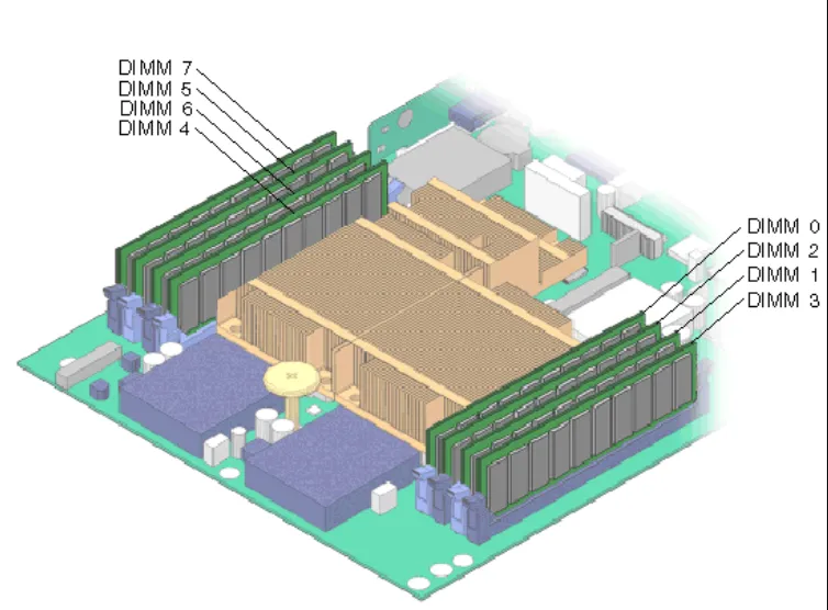
Why You Should Not Place Components Larger Than 3216 Directly Under a BGA