










PCB Edge Rails: Why Extra Edges Are Essential for Reliable SMT Handling
What This Video Covers
This video explains why PCB manufacturers intentionally add extra edges—known as edge rails—that are later removed after assembly. These rails are not part of the functional circuit. They create a solid, component-free zone that SMT conveyors use to grip and transport the board through the line. Without proper rails, conveyor tracks can strike components or cause the board to become unstable during high-speed placement.
The content covers practical design rules: rails must be added as a matching pair on two parallel opposite sides, typical widths of 5 mm (8 mm for large or high-density boards, never below 3 mm), and a minimum 1.0 mm component clearance from the future cut line. Fiducial marks and tooling holes are frequently placed on the rails for optical alignment and mechanical holding. After PCB assembly, the panel is separated by V-cut, mouse bites, or tab routing.
Engineers and buyers working on PCB prototypes or volume production will learn how correct rail design reduces handling defects and improves first-pass yield. For projects requiring precise panelization, request an instant PCB quote that already accounts for edge-rail requirements.
Key Highlights
- Edge rails create a mandatory component-free gripping zone so SMT conveyors can transport boards without striking parts or losing stability.
- Standard design practice uses 5 mm rails (increase to 8 mm for large or high-density boards; never go below 3 mm) with at least 1.0 mm component clearance from the cut line.
- Rails must be added as a parallel pair; after assembly the panel is separated by V-cut, mouse bites, or tab routing, and fiducials/tooling holes are commonly located on the rails themselves.
The Critical Role of Edge Rails in SMT Conveyor Handling
In modern SMT lines, boards travel on edge-supported conveyors. The conveyor rails or belts contact only the outer edges of the panel. Any component, solder pad, or copper feature in that contact zone risks mechanical damage, component tombstoning, or board drop-out. Edge rails solve this by providing a clean, solid strip of bare laminate (or laminate with only non-functional copper) that the machine can safely grip.
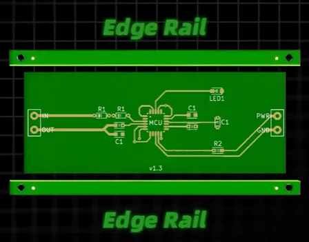
Factories observe that boards lacking adequate rails show higher rates of misplacement, solder-bridge defects from vibration, and occasional conveyor jams—especially on high-speed chip-shooters. The rails also stabilize the panel during reflow, reducing warpage-related coplanarity issues on larger panels.
Because the rails are sacrificial, they are designed out of the final product outline. This approach is standard across rigid FR4, multilayer, and many HDI constructions used in industrial control, automotive, and consumer electronics assemblies.
PCB Edge Rail Design Rules: Width, Placement, and Clearance
Rail width is the single most important geometric parameter. Industry practice and most contract manufacturers converge on these values:
| Board Characteristic | Recommended Rail Width | Notes |
|---|---|---|
| Standard size / normal density | 5 mm | Most common default |
| Large boards or high component density | 8 mm | Extra stiffness and grip area |
| Absolute minimum (tight panelization) | 3 mm | Risk of instability; confirm with assembler |
| Component keep-out from cut line | ≥ 1.0 mm | Prevents damage during V-cut or routing |
Rails must be placed as a matched pair on two parallel opposite sides so the conveyor can clamp both edges simultaneously. Placing rails on adjacent sides or only one side defeats the dual-edge gripping mechanism and is routinely rejected at DFM review.
Clearance rules are non-negotiable. Components, vias, or test pads closer than 1.0 mm to the intended separation line frequently suffer mechanical stress or copper tearing during depanelization. High-reliability applications (medical, automotive, aerospace) often increase this keep-out to 1.5 mm or more.
Fiducial Marks, Tooling Holes, and Depanelization Methods
Because the rails are outside the final board outline, they are ideal real estate for global fiducial marks and tooling holes. Optical systems use the fiducials for precise panel registration before placement begins; mechanical pins engage the tooling holes for secondary location or holding during selective soldering or conformal coating.

After SMT and any secondary processes, the panel is separated. Three common methods are used:
- V-Cut (score): fast and low-cost for straight edges; leaves a residual web that is snapped.
- Mouse bites (perforated tabs): good for irregular outlines; requires careful tab design to avoid stress concentration.
- Tab routing: full routing with small connecting tabs; offers the cleanest edge but higher machine time.
Choice of method influences residual stress, edge quality, and final dimensional tolerance. Incorrect rail design or inadequate clearance frequently causes copper peel or component damage at the separation step—problems that appear only after the expensive assembly process is complete.
FAQ
Q1: What is the minimum PCB edge rail width accepted by most SMT lines?
A1: Most contract manufacturers accept 3 mm as an absolute minimum, but 5 mm is the practical standard. Boards below 3 mm frequently experience conveyor instability or are rejected at incoming inspection.
Q2: Do all rigid PCBs require edge rails for SMT assembly?
A2: No. Very small boards, boards processed in carriers, or panels that already have sufficient unused edge area may omit dedicated rails. The decision depends on the specific SMT line configuration and the assembler's DFM rules. Always confirm before panelization.
Q3: How does edge-rail design affect depanelization cost and yield?
A3: Properly sized rails allow clean V-cut or tab routing with minimal stress. Undersized rails or insufficient component clearance increase scrap from edge damage and can force slower, more expensive routing methods, raising both cost and cycle time.
Q4: Where should fiducial marks and tooling holes be placed relative to edge rails?
A4: They are most commonly located on the rails themselves so they are removed after assembly and do not consume functional board area. Placement must still satisfy the optical system's field-of-view and minimum distance rules.
Q5: What clearance is required between components and the future cut line on edge rails?
A5: A minimum of 1.0 mm is required. High-reliability or high-density designs often specify 1.5 mm or greater to protect against mechanical stress during V-cut or mouse-bite separation.
Why do factories add extra board they're just going to cut off?
Those are Edge Rails. They're not part of the circuit.
In SMT the conveyor needs a solid, component-free zone to grip and move the board. Without them the tracks can hit parts or the board becomes unstable.
Fiducial Marks and Tooling Holes are often placed on these rails for alignment and holding.
Rails must be added as a pair on two parallel opposite sides so the conveyor can clamp properly.
Not every board needs them — it depends on the design and SMT line.
After assembly, the panel can be separated using V-Cut, mouse bites, or tab-routing.
Practical tip: use 5 mm rails. Go 8 mm for large or high-density boards, and never below 3 mm. Keep components at least 1.0 mm from the cut line.
Get the rails right, and assembly gets much easier.





