










Introduction
As electronic systems operate at higher frequencies, PCB signal loss impedance becomes a critical factor in ensuring reliable performance. Electrical engineers designing high-speed circuits must prioritize impedance control techniques to minimize signal loss and maintain signal integrity. Without proper control, mismatches lead to reflections, distortion, and reduced data rates in applications like telecommunications and computing. This article explores advanced strategies for low-loss PCB design, focusing on practical methods to optimize transmission lines. By understanding these principles, engineers can achieve consistent impedance across the board, reducing high-frequency signal loss effectively.
Understanding Impedance Control in PCBs
Impedance control refers to the process of designing PCB traces to maintain a specific characteristic impedance, typically 50 ohms for single-ended lines or 100 ohms for differential pairs. This characteristic impedance arises from the interaction between inductance and capacitance in the transmission line structure. In PCBs, factors such as trace width, thickness, dielectric height, and material properties dictate the impedance value. Proper control prevents signal reflections at interfaces, which degrade quality and contribute to PCB signal loss impedance issues. For high-speed signals, even small deviations can amplify losses over long traces. For foundational concepts, refer to our guide on Signal Integrity and Impedance Control: Transmission Line Theory.
The relevance of impedance control intensifies with rising clock rates in modern electronics. High-frequency signal loss manifests as attenuation and phase shifts, limiting bandwidth and eye diagram opening. Engineers must consider both return loss from mismatches and insertion loss from material dissipation. Standards like IPC-2141A provide guidelines for calculating and verifying controlled impedance in high-speed designs. Implementing these ensures compliance and optimal performance across manufacturing variations.
Key Mechanisms of Signal Loss in High-Frequency PCBs
Signal loss in PCBs primarily stems from conductor losses, dielectric losses, and radiation effects, all exacerbated at high frequencies. Conductor losses dominate due to the skin effect, where current flows near the conductor surface, increasing effective resistance. Surface roughness on copper further elevates this loss by scattering the current path. Dielectric losses occur as the insulating material absorbs energy, quantified by its dissipation factor. Together, these mechanisms cause exponential attenuation with frequency, making minimizing signal loss a priority in low-loss PCB design.
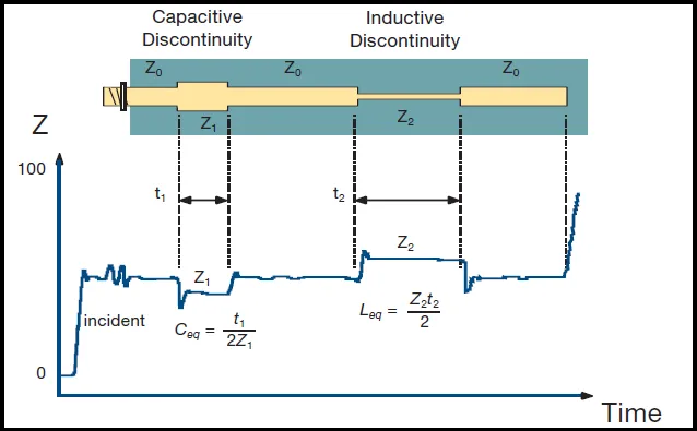
Transmission line theory underpins these losses, modeling traces as distributed RLC networks. Reflections occur when impedance discontinuities disrupt wave propagation, quantified by the reflection coefficient. Radiation losses arise from unbalanced fields or sharp bends, coupling energy away from the signal path. High-frequency signal loss also includes connector and via contributions, which introduce parasitic inductance and capacitance. Understanding these interactions allows engineers to target specific impedance control techniques for mitigation.
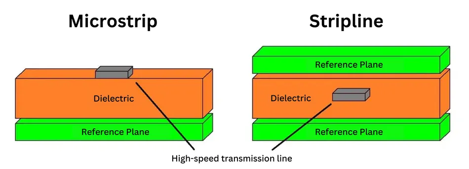
Dielectric properties play a pivotal role, with relative permittivity influencing capacitance and thus impedance. Variations in dielectric constant across the board lead to inconsistent Z0, promoting crosstalk and loss. Thermal expansion differences between layers can warp the structure, altering dielectric spacing post-fabrication. Engineers must model these effects during design to predict real-world behavior accurately.
The table below summarizes these mechanisms:
| Mechanism | Primary Cause | Impact on High-Frequency Signal Loss | Mitigation Strategy |
|---|---|---|---|
| Conductor (Skin Effect + Roughness) | Current crowding + surface texture | Dominant above 5 GHz; up to 50 % of total loss | Smooth copper foils (HVLP), wider traces |
| Dielectric Losses | Material Df and frequency dependence | Increases linearly with frequency | Low-Df laminates (Rogers, Megtron, Tachyon) |
| Radiation | Discontinuities, poor return paths | Energy leakage, EMI | Continuous reference planes, stitching vias |
| Via/Connector Parasitics | Stub inductance, impedance mismatch | Resonant notches, reflections | Backdrilling, blind/buried vias |
Factors Influencing PCB Impedance
Several geometric and material parameters determine trace impedance in PCB layouts. Trace width directly affects inductance, while height to the reference plane governs capacitance. Copper thickness impacts both, especially in thin high-frequency traces. Dielectric materials with stable permittivity ensure predictable Z0 across temperature and frequency ranges. Symmetric stackups minimize intra-layer variations, supporting uniform impedance control techniques.
Fabrication tolerances introduce variability, such as etching undercuts reducing effective width or plating adding thickness. Reference plane splits or voids create return path discontinuities, spiking impedance. Via stubs act as resonators, reflecting signals at quarter-wave frequencies. Engineers address these through design rules that incorporate statistical margins for manufacturing.
Advanced Techniques for Impedance Control and Loss Minimization
Material selection forms the foundation of low-loss PCB design, favoring dielectrics with low dissipation factor and stable dielectric constant. These materials reduce energy absorption, crucial for high-frequency signal loss reduction. Low-profile copper foils minimize surface roughness, lowering conductor losses via smoother current flow. Combining these yields lower insertion loss over multi-gigabit links.
Trace geometry optimization involves precise width and spacing calculations based on stackup specifics. Microstrip lines suit outer layers for easier routing, while striplines offer better shielding in inner layers. Differential pairs require tight length matching to preserve common-mode rejection. Adhering to IPC-2221 design standards ensures traces meet current and thermal requirements alongside impedance targets. Proper layer arrangement is critical; see our comprehensive guide on Optimizing PCB Stackup for High Speed Signals.
Routing strategies further enhance minimizing signal loss. Length-matched serpentine routes equalize delays in differential signals. Avoiding right-angle bends reduces radiation and stub effects; use 45-degree miters instead. Proximity to reference planes must remain constant, with ground vias stitching planes to contain fields. These impedance control techniques collectively suppress crosstalk and attenuation.
Via design innovations tackle high-frequency bottlenecks. Backdrilling removes stubs, preserving signal fidelity beyond 10 GHz. Blind or buried vias shorten paths, reducing parasitic effects. Controlled depth drilling aligns with layer targets, maintaining stackup integrity. Simulation verifies these before fabrication, correlating with time-domain reflectometry measurements.
Power plane partitioning isolates noisy sections, stabilizing reference potentials. Decoupling capacitors near ICs provide low-impedance return paths. Fill stitching connects plane fragments, minimizing impedance spikes. These practices integrate seamlessly into overall low-loss PCB design workflows.
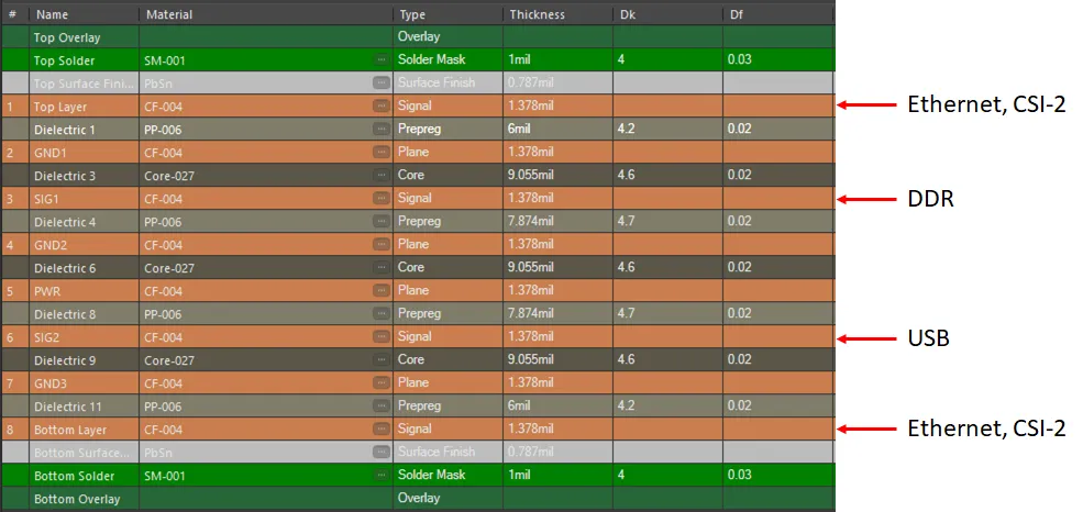
PCB Stackup Design for Controlled Impedance
PCB stackup design is one of the highest-leverage decisions in pcb impedance control. A symmetric, balanced construction (equal copper distribution and dielectric thicknesses above and below the centerline) minimizes warpage and keeps dielectric spacing consistent.
Recommended practices:
- Place critical high-speed layers adjacent to solid reference planes with dielectric height chosen for target Z0 (typically 4–10 mil for 50 Ω).
- Use low-Dk, low-Df cores and prepregs throughout high-speed zones; hybrid stacks (standard FR-4 outer + low-loss inner) can reduce cost when routed carefully.
- Allocate at least one continuous ground plane adjacent to every signal layer; avoid splits under high-speed traces.
- For 8–16 layer boards common in data-center designs, interleave signal and plane layers to achieve both routing density and signal integrity.
Example 8-layer stack: Signal/GND/Signal/PWR//PWR/Signal/GND/Signal with tight-tolerance Megtron 6 dielectrics yields tightly controlled 50 Ω single-ended and 100 Ω differential pairs with < ±5 % variation.
Troubleshooting Common Impedance Issues
Engineers often encounter impedance drifts from fabrication variances, detectable via TDR scans. Warpage alters dielectric spacing, shifting Z0; controlled lamination per IPC-6012E specifications mitigates this. Moisture absorption swells dielectrics, increasing capacitance; bake-out processes stabilize boards pre-assembly.
Crosstalk troubleshooting involves spacing analysis and guard traces. Simulations reveal coupling levels, guiding layout revisions. Post-fab coupons embedded in panels allow direct impedance verification. Iterative design cycles refine these, ensuring production yields meet specs. Combine TDR analysis with best practices from our article on PCB Impedance Control and EMI Reduction.
Fabrication Considerations and Test Coupons
Fabrication directly affects final controlled impedance. Specify impedance tolerances (±10 % standard; ±5 % for premium high-speed designs) on drawings and require test coupons in every panel.
Coupons should include representative traces (single-ended and differential) on every critical layer, with identical copper weight and dielectric configuration. Fabricators use TDR or capacitance testing on coupons; request test reports.
Key considerations: control etch factor, copper roughness, resin content, and lamination pressure to minimize Dk variation. IPC-6012 and IPC-2141A provide acceptance criteria. Choose suppliers experienced with low-loss materials like Rogers or Megtron and request “impedance-first” process controls.
Case Studies and Real-World Examples
Case 1 – 28 GHz 5G Antenna Module
A telecom customer experienced excessive insertion loss (>1.2 dB/inch at 28 GHz). Switching from standard FR-4 to Rogers RO4350B with HVLP copper and implementing backdrilled vias reduced loss to 0.45 dB/inch. PCB stackup design was symmetrized and verified with VNA, improving link budget by 3 dB and eliminating a planned respin.
Case 2 – 112 Gbps AI Server Backplane
Intermittent eye closure was traced via TDR to via stubs and plane voids under high-speed lanes. Redesign with blind vias, continuous reference planes, and Megtron 8 material, combined with tighter length matching, opened the eye by 35 % and raised yield from 76 % to >98 %.
Case 3 – 77 GHz Automotive Radar
Warpage after reflow shifted impedance on critical RF traces. A hybrid stack with low-CTE low-loss laminates, tighter lamination controls per IPC-6012, and embedded test coupons brought impedance variation within ±4 %. Field failure rate dropped dramatically.
These examples demonstrate the ROI of investing early in rigorous pcb impedance control and low-loss pcb design.
Conclusion
Mastering advanced PCB impedance control techniques is essential for electrical engineers tackling high-speed challenges. By addressing conductor and dielectric losses through material choices, precise geometries, and routing discipline, significant reductions in PCB signal loss impedance occur. Standards like IPC-2141A and IPC-2221 guide these efforts, promoting reliable low-loss PCB design. Implementing simulation, verification, and troubleshooting ensures robust performance. Ultimately, these strategies enable higher data rates and system margins in demanding applications.
FAQs
Q1: What causes PCB signal loss impedance in high-frequency designs?
A1: PCB signal loss impedance arises mainly from mismatches causing reflections, alongside conductor losses from skin effect and dielectric absorption. Surface roughness and via parasitics compound attenuation at gigahertz frequencies. Engineers mitigate this via controlled trace geometries and low-loss materials. Proper stackup symmetry prevents variations, ensuring consistent performance across the board.
Q2: How do impedance control techniques minimize signal loss?
A2: Impedance control techniques minimize signal loss by matching characteristic Z0 to source and load, eliminating reflections and return loss. Low-profile copper and low-Df dielectrics reduce insertion loss components. Symmetric routing and backdrilled vias preserve signal integrity. Verification with TDR confirms tolerances, aligning design with fabrication realities.
Q3: What role does stackup design play in low-loss PCB design?
A3: Stackup design in low-loss PCB design dictates dielectric spacing and plane proximity, directly influencing trace capacitance and inductance. Uniform thicknesses ensure predictable impedance across layers. Reference planes shield signals, curbing radiation losses. Engineers optimize for high-frequency signal loss by balancing symmetry and layer count.
Q4: Why is surface roughness critical for high-frequency signal loss?
A4: Surface roughness increases effective conductor resistance at high frequencies due to current crowding in peaks. Smoother profiles, like reverse-treated foil, lower skin effect losses significantly. This enhances overall minimizing signal loss efforts in impedance-controlled traces. Fabrication processes must prioritize profile control for optimal results.
References
IPC-2141A — Design Guide for High-Speed Controlled Impedance Circuit Boards. IPC
IPC-2221 — Generic Standard on Printed Board Design. IPC
IPC-6012E — Qualification and Performance Specification for Rigid Printed Boards. IPC, 2015






