


PCB Specifications
| Parameter | Value | Parameter | Value |
|---|---|---|---|
| PCB Type | Copper Core PCB | Quantity | 5 pcs |
| Layers | 1 Layers | Board Type | Panel PCB |
| Dimensions | 123.2 x 83.8 mm | Copper Weight | 2oz |
| Thickness | 2 mm | Min Track / Spacing | 5/5mil |
| Surface Finish | OSP | Min Hole Size | 1.2mm |
| Solder Mask | Matte Black | Silkscreen | None |
| Thermal Conductivity | 380W |
Manufacturing Timeline
Logistics Information
Key Manufacturing Processes
Manufacturing Summary
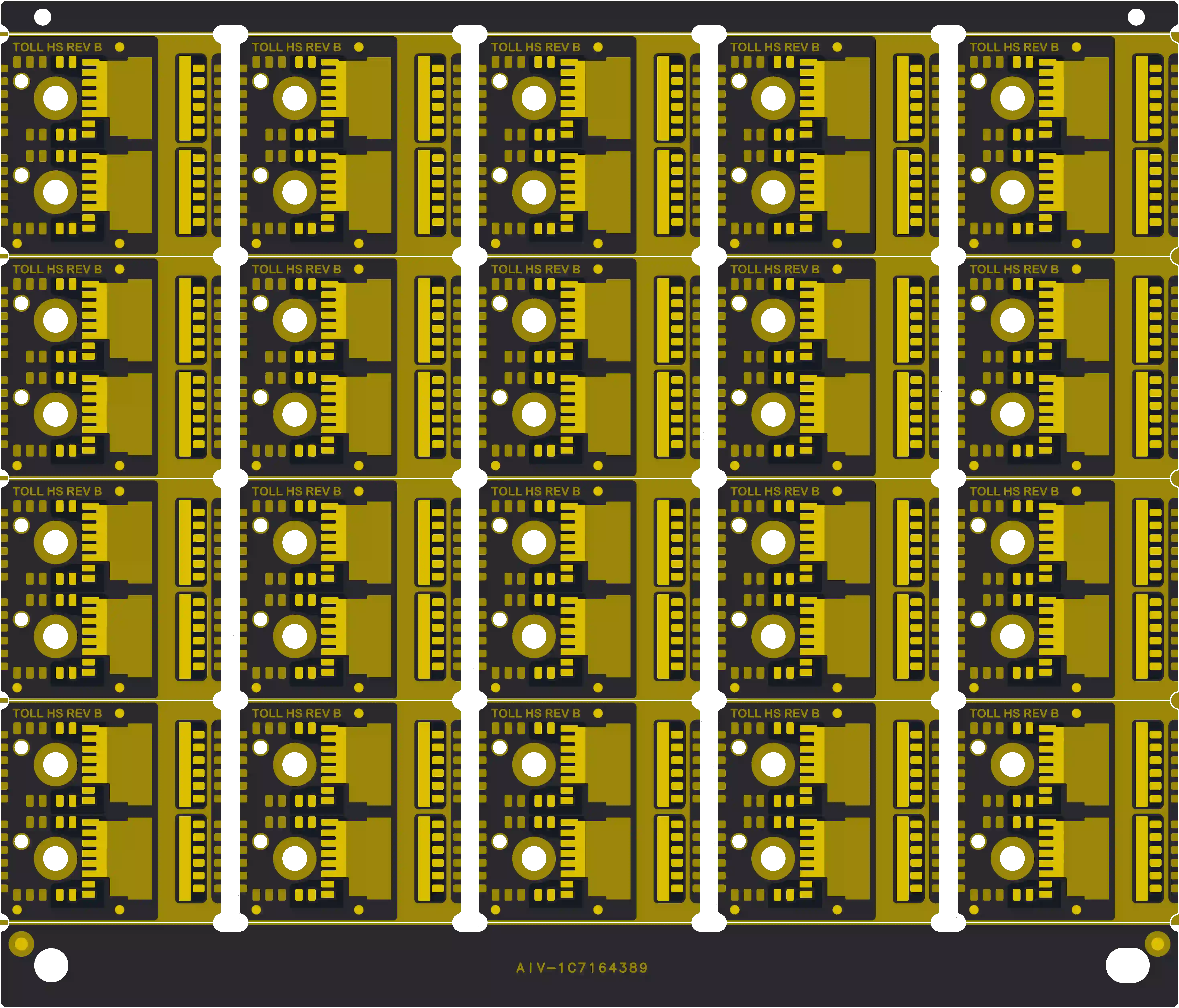
This order consisted of five single-layer copper core PCBs produced as panels, each measuring 123.2 × 83.8 mm with a total thickness of 2 mm. The 380 W/mK copper core required dedicated material preparation, copper core processing, and thermal via implementation to ensure effective heat dissipation. Base 2 oz copper was supplemented with thick copper electroplating and controlled etching to accurately produce the 5/5 mil track and spacing on this heavier copper design.
Matte black solder mask was applied without silkscreen, followed by OSP surface finish and anti-oxidation treatment to protect the exposed copper. These steps, together with precise plating control, preserved feature integrity across the panels while meeting the specified tolerances for this copper core PCB. Full electrical testing confirmed circuit continuity and isolation on every board.
The complete sequence from engineering review through heavy copper plating and final inspection extended over 12.2 days. Attention to etching uniformity and thermal via plating delivered consistent thermal performance and mechanical stability suited to high-power applications.
Explore More PCB Manufacturing Resources

Copper Core PCB Manufacturing Insights
Copper core PCBs deliver high thermal conductivity for power applications. Manufacturing emphasizes reliable core bonding and precise via formation.
Stackup and Gold Thickness Limits in Thermoelectric Separation Copper Base PCBs
This technical assessment examines manufacturing capability for thermoelectric separation copper base PCBs. It focuses on the decision to adopt conventional stackup over customer documentation and the resulting 0.05µm ENIG gold thickness limit caused by direct connection between edge pads and base copper, while maintaining 380W thermal conductivity and insulation performance.
Real Production Records
| Order ID | PCB Type | Layers | Dimensions | Solder Mask | Surface Finish | Quantity | Action |
|---|---|---|---|---|---|---|---|
| CU-20261008-082 | Copper Core PCB | 1 | 110 x 84 | Warm White | OSP | 30 | View detail |
| CU-20260923-045 | Copper Core PCB | 1 | 29 x 20 | Warm White | OSP | 20 | View detail |
| CU-20260720-048 | Copper Core PCB | 1 | 100 x 84 | Warm White | OSP | 10 | View detail |


