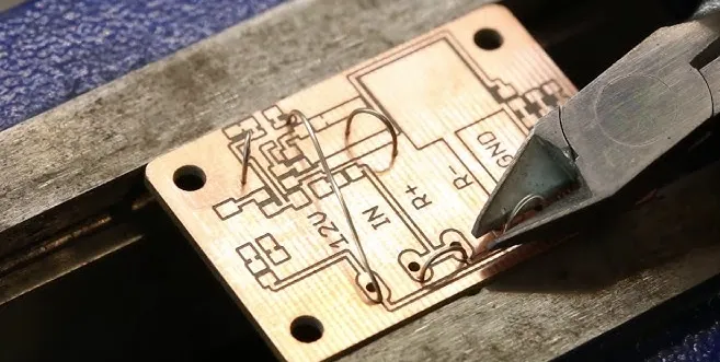
Via Plating
Via plating is a critical process in printed circuit board (PCB) manufacturing that involves depositing a conductive layer, typically copper, inside the drilled holes known as vias. These vias serve as essential interconnections between different layers of a multilayer PCB, enabling reliable signal transmission and power distribution. For engineers, designers, and hobbyists searching for information on via plating, this tag aggregates in-depth articles that explore the techniques, materials, and standards involved in achieving high-quality plating results. Understanding via plating helps prevent common issues like voids, insufficient thickness, or poor adhesion, which can lead to electrical failures or reduced board longevity. In practice, via plating enhances PCB performance by ensuring low-resistance paths and improving thermal management, especially in high-density designs used in consumer electronics, automotive systems, and telecommunications equipment. Key best practices include selecting appropriate plating chemistries, such as electroless copper followed by electrolytic deposition, and adhering to IPC standards for thickness and uniformity. Actionable insights from our articles cover optimizing via aspect ratios to avoid plating defects, troubleshooting barrel cracking during thermal cycling, and integrating via plating into automated manufacturing workflows. For instance, designers can apply these principles to minimize signal integrity problems in high-speed circuits or enhance reliability in harsh environments. By delving into the content under this tag, readers gain practical knowledge to refine their PCB fabrication processes and innovate in electronics design. Related articles discuss advanced topics like blind and buried vias, alternative plating materials for lead-free compliance, and cost-effective strategies for prototyping, providing a comprehensive resource for both beginners and seasoned professionals.
Technical Articles
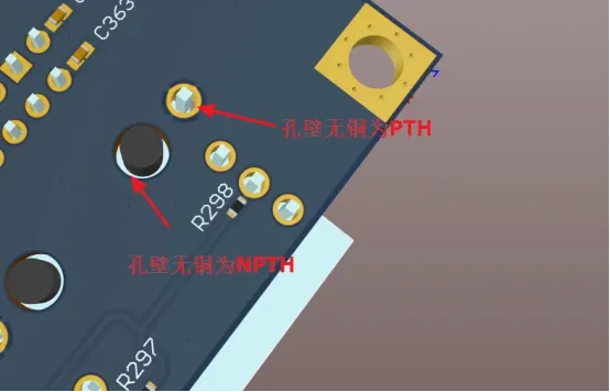
PTH and NPTH on a PCB: How to Tell the Holes Apart
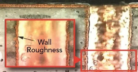
What Causes PCB Barrel Copper Separation?

8-Layer PCB Reliability: Common Failure Modes and Design Considerations

IPC-4761: PCB Via Protection Types and Design Considerations
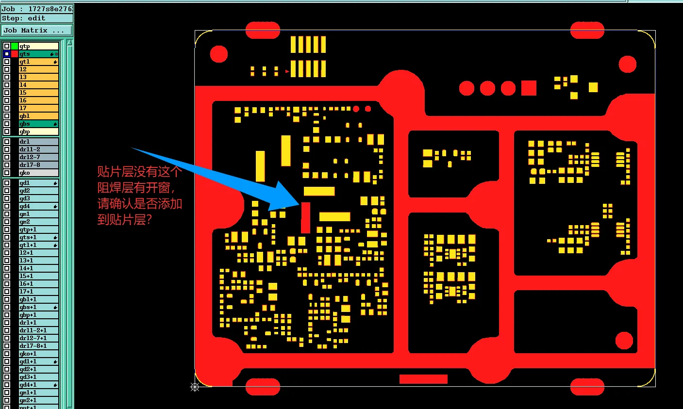
How to Prevent Buried Via Plating and Stackup Mismatch Issues in 8-Layer TG170 PCB
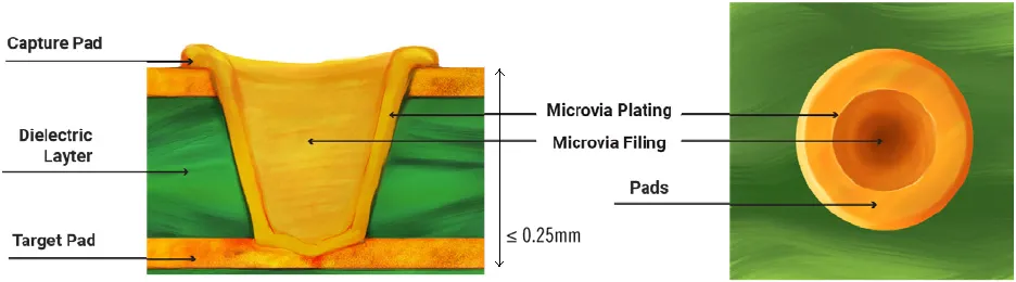
High Aspect Ratio PCBs: Challenges, Solutions, and Advanced Manufacturing Techniques
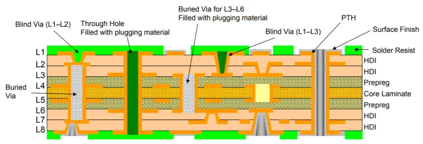
PCB Aspect Ratio and Thermal Management: Keeping Your Boards Cool and Reliable
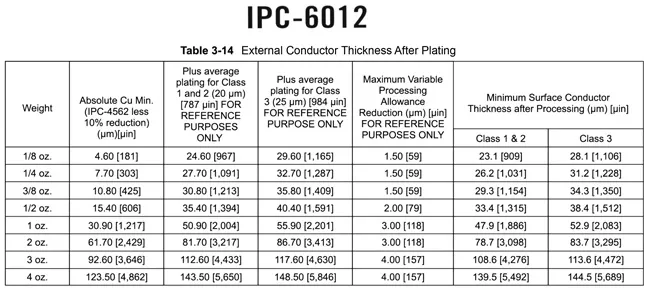
IPC-6012 Standard: Hole and Via Plating Thickness Requirements
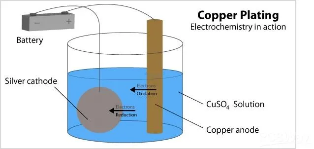
Electroless vs. Electrolytic Plating: Which Method is Right for Your PCB?
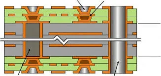
The Ultimate Guide to Stacked Via Aspect Ratio: Balancing Performance and Manufacturability
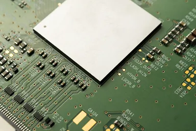
How to Choose the Right Blind Via Diameter for HDI PCB
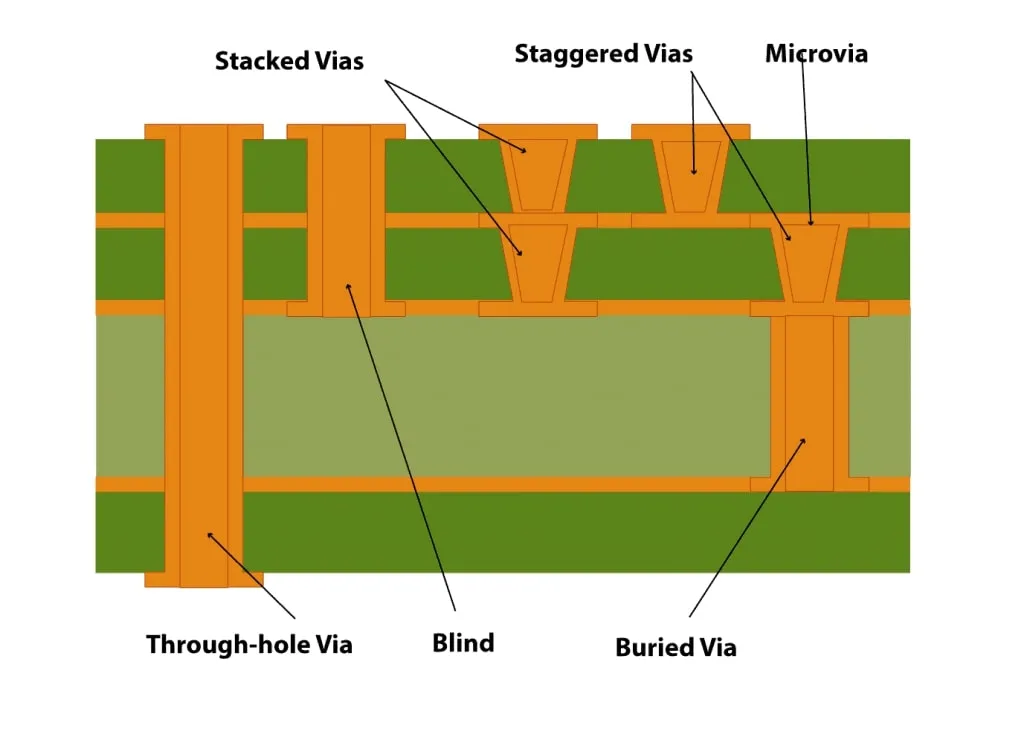
Best Practices for Plating Stacked Vias: Achieving Uniform Copper Deposition
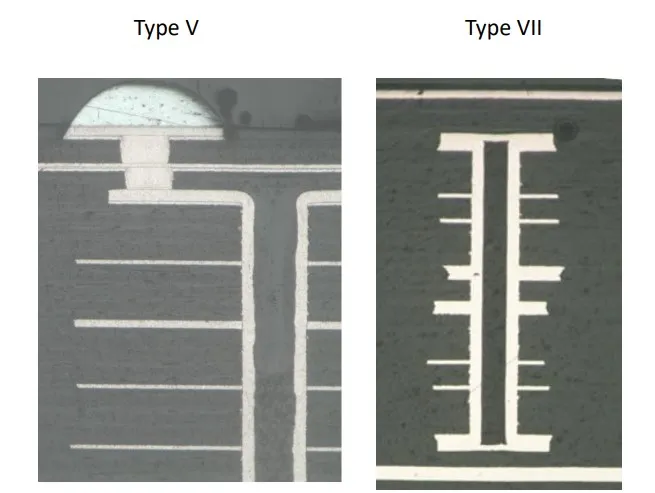
Troubleshooting Via Filling Defects: Identifying and Resolving Common Issues
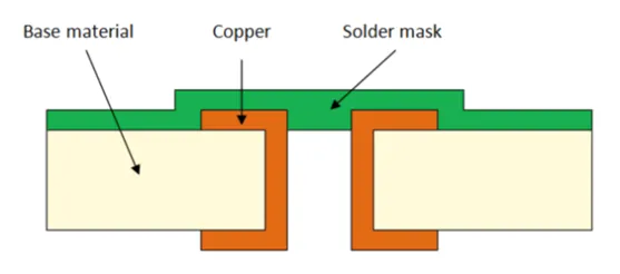
PCB Via Plating: Process, Methods, and Thickness Requirements
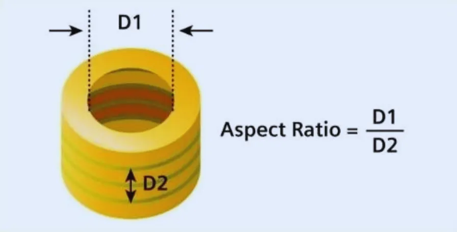
Ensuring PCB Reliability: The Crucial Role of Via Aspect Ratio
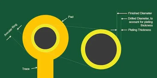
FR4 PCB Via Size and Pad Size: How to Choose the Right Dimensions
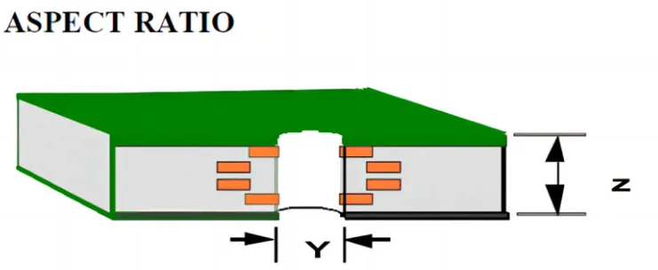
FR4 PCB Hole Aspect Ratio: Why It Matters for Plating Reliability
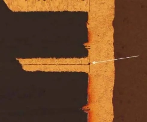
FR4 PCB Plated Through-Hole Reliability: Common Risks and Controls