










In production we treat FR4 PCB plated through hole reliability as a process window that has to be locked early, not something we try to recover later. CAM engineers set the minimum average copper in the hole wall at 20–25 µm depending on class, keep the aspect ratio under control, and require full desmear plus electroless copper coverage before any electrolytic plating starts. Boards that come in with high aspect ratios or thin final copper are flagged at DFM and either compensated with adjusted plating parameters or returned for redesign. That is the baseline we run every FR4 job against.
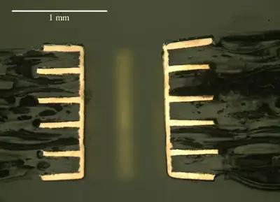
Where Z-axis expansion and plating thickness start fighting each other
FR4 resin expands in the Z direction at roughly 50–70 ppm/°C while the copper barrel sits at 17 ppm/°C. Every time the panel goes through lamination cool-down, solder-mask cure, or the customer’s reflow profile, the resin tries to stretch the copper. If the copper is thin, discontinuous, or poorly adhered after drilling smear, the stress concentrates at the knee of the hole and at the mid-barrel. What we typically see on the CAM side is that designers specify finished hole size but leave the plating thickness and aspect ratio as afterthoughts. Once the panel is drilled and the hole wall is rough or resin-smeared, electroless copper cannot deposit evenly and the electrolytic copper builds thinner at the center of high-aspect holes. That is the point where PTH reliability FR4 PCB starts to become a real production risk rather than a drawing note.
Drilling parameters also force the issue. Dull bits, high feed rates, or inadequate chip evacuation leave smear and glass fiber protrusion. Desmear chemistry has to remove that layer without attacking the copper pads or undercutting the resin. If the desmear is light, the electroless step plates over residual smear; if it is aggressive, the hole wall becomes too rough and traps voids. Either way the copper-to-resin interface is weakened before the board ever sees thermal cycling.
What actually fails when hole-wall copper is left marginal
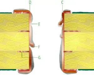
Boards that leave the factory with average wall copper below 18 µm or with voids at the knee routinely show barrel cracks after one or two thermal-shock cycles. The crack usually starts at the outer corner of the pad-to-barrel junction and propagates inward until the circuit opens. In extreme cases the copper separates from the resin wall and the hole becomes an intermittent contact that only fails after the customer has already assembled the board. Yield impact shows up first in the microsection lab: we reject panels when more than one hole in a five-hole sample set fails the thickness or continuity criteria. If the problem is systemic, the entire lot is held, reworked if possible, or scrapped. Shipment delays of one to two weeks are common when plating chemistry or current-density settings have drifted and the defect is only caught at final inspection.
Assembly houses see the same boards as open circuits after reflow or as intermittent failures in the field. Because the damage is internal, optical inspection and flying-probe tests often pass the bare board, so the failure travels downstream. That is why we treat FR4 PCB plated through hole reliability as a process-control metric rather than a final-test metric.
Process locks we put on every FR4 PTH job
Most factories handle this by fixing three numbers and one process sequence. First, finished copper in the hole wall is specified as 20 µm minimum average for Class 2 and 25 µm for Class 3, measured at the thinnest point of the barrel after etching. Second, aspect ratio is limited to 8:1 for standard vertical plating lines; anything higher requires pulse plating or panel redesign. Third, electroless copper thickness is held above 0.5 µm with full coverage verified by backlight or microsection before electrolytic plating begins.
On the CAM side we adjust the drill size so that after plating and etch the finished hole meets the drawing while still allowing enough copper. Panel plating current density is kept in the 1.5–2.5 ASD range and agitation is increased for high-aspect panels. Desmear dwell time and temperature are locked to the specific FR4 resin system; we do not run a universal cycle. After plating, every production lot gets a five-hole microsection sample checked for thickness, voids, and adhesion. If any sample fails, the lot is stopped and the plating bath is analyzed for brightener and chloride levels before the next panel is released.
These steps exist because the copper barrel is the only continuous electrical path through the board. Once the panel is laminated and soldermask is applied, there is no practical way to thicken the hole wall again. Controlling the process upstream is cheaper than sorting failed assemblies downstream.
When we can loosen the copper target without raising risk
Boards with aspect ratios below 4:1, four layers or fewer, and no high-temperature assembly cycles can run with 15–18 µm average wall copper if the customer accepts Class 2 electrical requirements only. In those cases we still keep full desmear and electroless coverage, but we drop the electrolytic plating time. The trade-off is lower current-carrying capacity and reduced thermal-cycle life; we note both on the traveler so the customer sees the limit. High-reliability or automotive jobs stay at the full 25 µm target regardless of layer count. Anything between those extremes is negotiated case by case at the DFM stage, never on the plating line.






