In production we handle FR4 PCB drilling by treating finished hole diameter as a target that is never drilled directly. CAM engineers take the design finished size, add plating allowance and process compensation, then generate the drill program with that adjusted diameter. Typical compensation on standard FR4 is 0.08–0.15 mm over the finished hole, depending on copper weight, aspect ratio and whether the hole is plated-through. Spindle speed, feed rate and hit count limits are locked to the smallest hole and thickest stack in the panel before the job is released to the drill floor.
What we typically see on the CAM side is a diameter table that already accounts for average plating thickness of 20–30 µm per wall plus the expected bit wear after a set number of hits. Entry aluminium and exit material are called out in the same program so the first board and the last board stay inside the same tolerance band. That is the baseline control method for FR4 hole drilling across most production panels.
Why glass weave and resin heat force diameter movement during FR4 PCB drilling
FR4 forces the problem because the material itself changes under the drill. The woven glass fabric is abrasive; after a few thousand hits the effective bit diameter drops by 10–20 µm even when the spindle is still within life limits. At the same time the resin softens from frictional heat, especially once board thickness exceeds 1.6 mm or the aspect ratio climbs above 8:1. Softened resin smears on the hole wall and then re-hardens, so the measured diameter after drilling is smaller than the programmed size.
Machine positioning tolerance stacks on top of that. A typical multi-spindle drill holds ±0.05 mm positional accuracy under ideal conditions, but panel expansion from moisture and temperature, plus the cumulative error from pin registration, routinely pushes the real hole location another 30–50 µm off the pad centre. When the same panel also carries holes of different sizes, the smaller bits run at higher RPM and generate more heat, so diameter drift is never uniform across the panel. That combination of bit wear, resin smear and registration stack-up is why hole-size control cannot be left to the design file alone.
What uncontrolled hole size does to annular ring and downstream yield
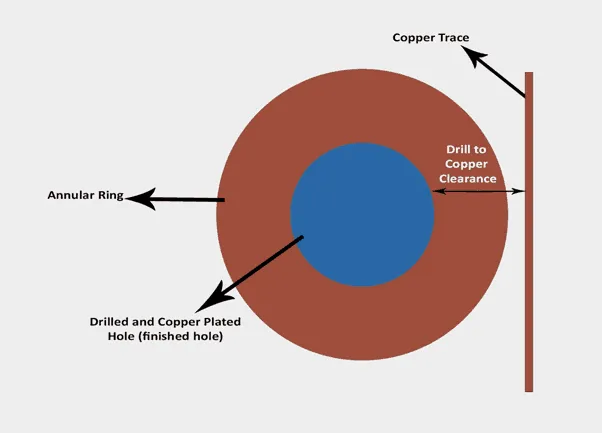
If the compensation is wrong or the bit is left running past its life limit, the finished hole after plating lands outside the customer tolerance. Undersize holes reject press-fit connectors or cause solder-joint stress at assembly. Oversize holes eat into the annular ring; once the remaining copper is less than 0.05 mm the risk of open circuits after thermal cycling rises sharply. On dense boards the same positional drift that starts as a 0.07 mm shift becomes a breakout that forces the panel into scrap.
Bit breakage mid-panel is the other common outcome. A worn bit seizes in a thick FR4 stack, the spindle stalls, and the remaining holes on that panel are either missing or drilled with a replacement bit that has a different effective diameter. The panel then has mixed hole sizes, which plating cannot correct. Yield drops of 5–15 % on high-density jobs are typical when diameter control is left to the operator instead of the CAM program. Shipment delays follow because the panel has to be re-drilled or rejected and re-started.
How CAM diameter tables and process parameters keep FR4 holes inside tolerance
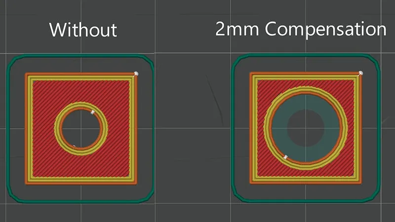
Most factories solve the issue by locking compensation into the drill program before any board is loaded. CAM engineers maintain a diameter table keyed to copper weight, board thickness and plating type. For a standard 1 oz copper, 1.6 mm FR4 PTH hole the program drills 0.10–0.13 mm larger than the finished size; for 2 oz copper the oversize increases by another 0.02–0.03 mm. The same program sets spindle speed and feed according to the smallest hole present: 0.2 mm bits typically run at 100–120 krpm with reduced chip load, while 0.5 mm bits drop to 60–80 krpm.
Entry aluminium (0.15–0.2 mm) and exit phenolic or cardboard are mandatory on every panel. They stabilise the bit on entry and prevent resin breakout on exit, which keeps the top and bottom diameters matched. For aspect ratios above 10:1 we switch to peck drilling—two or three controlled depth steps—so heat does not build up and smear the wall. Vacuum pressure and spindle air are monitored in real time; if either drops the machine stops the hit count and flags the bit for replacement.
After the first panel, sample holes are measured with pin gauges or an optical system. If the average diameter has moved more than 15 µm from the programmed value, the CAM table is adjusted for the rest of the lot and the bit life limit is tightened. On critical jobs an X-ray registration check is added before plating so any positional drift can still be caught while the copper is still available for compensation. These steps keep the FR4 PCB drilling process inside the normal ±0.05 mm or ±0.075 mm finished-hole window without relying on operator judgement.
When larger holes and low-density layouts let us relax the controls
Exceptions are allowed when the smallest finished hole is 0.5 mm or larger and the board is two- or four-layer with generous annular rings. In those cases the diameter compensation can be reduced to 0.05–0.08 mm and bit life extended by 30–50 %, because wear and smear have far less impact on the final size. Prototype runs with loose customer tolerances can also drop the optical first-article measurement and run on standard parameters. The trade-off is clear: once hole density rises or the aspect ratio exceeds 8:1 the same relaxation quickly produces out-of-spec annular rings and the panel is back under full control.