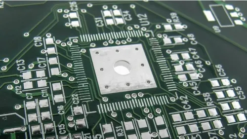
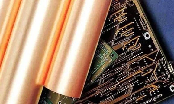
In production we treat HDI laser drilling defects as a process window problem, not a one-off machine fault. CAM engineers set the laser recipe against the actual dielectric stack and copper thickness before the panel ever reaches the laser station. When the design calls for 75 µm or smaller microvias in RCC or thin ABF, we lock pulse energy, repetition rate, and focus offset to a narrow band that has already been qualified on the same material lot. Any deviation outside that band is rejected at first-article inspection rather than corrected downstream.
Where the defect modes actually show up on the laser line
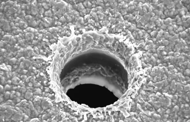
The six defects we see most often are aperture out-of-spec, non-round hole shape, residual dielectric at the pad, sidewall carbonization, positional shift, and wall roughness or micro-cracks. Aperture growth or shrinkage usually tracks total energy density. Too many pulses or higher peak power opens the top diameter beyond the ±10 µm window most HDI customers accept. Too little energy leaves the bottom diameter undersized and the via incomplete. Non-round shape appears when the laser beam is slightly elliptical or the galvanometer scan path drifts; the hole then becomes oval along the scan axis. Residue at the bottom is incomplete ablation—common when the dielectric thickness varies across the panel or the copper pad reflectivity changes after previous processes. Carbonization shows as blackened sidewalls and is driven by residual heat that exceeds the decomposition temperature of the resin. Positional offset is almost always registration: either the laser camera cannot lock to the target fiducials or the panel expands differently from the compensation table. Wall damage—roughness or micro-cracks—occurs when the pulse energy is high enough to ablate but the heat-affected zone reaches into the glass or filler particles.
Material behavior forces most of these defects into existence. RCC and ABF both contain inorganic fillers whose ablation threshold is higher than the surrounding resin. Once the resin is gone the fillers remain as protrusions or scatter the next pulse, leaving an irregular wall. Copper thickness under the via also matters: 12 µm foil absorbs differently from 18 µm, so the same recipe that cleans a thin pad leaves residue on a thicker one. Panel moisture content after bake is another variable; even 0.1 % residual moisture turns into vapor that disrupts the plasma and leaves carbon or residue.
What the line produces when the process window is ignored
Uncontrolled HDI laser drilling defects translate directly into yield loss at electrical test and later reliability failures. Undersized or residue-filled vias fail continuity after plating; the copper cannot nucleate on residual dielectric and the via stays open. Oversized vias reduce annular ring and can undercut the capture pad, causing open circuits after thermal stress. Carbonized walls plate poorly—the carbon acts as a barrier—so the plated copper is thin or discontinuous. Positional shift of more than 25 µm moves the via off the target pad and creates either a partial open or a short to adjacent circuitry once the board is assembled. Rough or cracked walls trap plating chemistry, leading to voids that grow under reflow and fail in the field. On a typical 4-layer HDI panel these defects can drop first-pass yield by 8–15 % if the laser recipe is not locked; the scrap is usually discovered only after plating and AOI, so the material and process cost is already sunk.
How the factory keeps the defects inside the process window
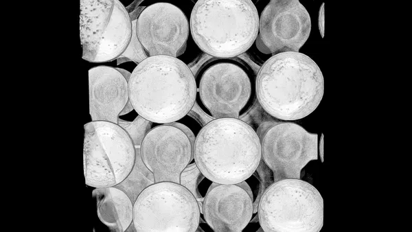
We control HDI laser drilling defects first in CAM and then on the machine. CAM engineers extract the exact dielectric thickness and copper weight from the stack-up and select a qualified recipe from the laser database. That recipe fixes pulse energy (typically 0.8–1.6 mJ for UV lasers on ABF), pulse count (8–20 pulses for 60–80 µm vias), and focus offset relative to the top copper surface. Before production starts we run a first-article panel, measure via diameter at top and bottom with an optical microscope or laser confocal system, and check registration to the target pads. If any dimension is outside the customer tolerance we adjust energy or focus by 5 % steps and re-qualify. On the production laser we keep the beam profile circular by daily galvanometer calibration and we verify fiducial recognition accuracy to ±5 µm. Panel bake is mandatory—usually 1–2 hours at 120 °C—to drive residual moisture below 0.05 %. After drilling we run a plasma or chemical desmear to remove any residual carbon and to micro-etch the copper pad so plating can start cleanly. In-process AOI after laser and again after plating catches residual defects before they leave the factory.
Design-side choices directly affect how tight that window becomes. Via diameters below 60 µm on thick dielectric force higher energy and therefore more carbon risk. Capture pads smaller than 150 µm leave little margin for the 20–25 µm registration tolerance most lasers achieve on large panels. Uneven copper distribution around the via array changes local thermal mass and can shift the effective ablation threshold from one location to another. When the design keeps via size, pad size, and dielectric thickness inside the ranges we have already qualified, the same recipe runs stably across an entire lot.
Cases where we can relax the normal controls
We allow wider process windows when the vias are larger than 100 µm, the dielectric is thin RCC, and the board is not going into high-reliability applications. In those cases a ±15 µm diameter tolerance and ±30 µm registration are acceptable, and we can run a single-pass recipe without intermediate measurement. Prototypes that will see only limited thermal cycling can also skip the full first-article qualification if the customer accepts the risk. Outside those conditions the normal parameter lock and inspection steps stay in place; the cost of an uncontrolled defect later in the flow is higher than the time spent keeping the laser inside its window.