In production, most HDI CAM review changes start the moment the stack-up and laser via data hit the CAM station. We do not wait for a formal DFM report. The first pass is a hard check against our process windows for microvia aspect ratio, residual copper after sequential plating, and cumulative registration through every lamination cycle. If the design exceeds those windows, we either enlarge the capture pad, shift the via position within the available annular ring, or request a stack-up revision before the job ever reaches the laser drill. That is the normal entry point for HDI CAM review changes.
What we typically see on the CAM side is a design that looks clean on the designer's screen but already sits outside the real capability of sequential build-up. Laser drill accuracy is ±25 µm on a good day; after two or three press cycles the material movement and copper thickness variation push the true registration stack beyond that. When the designer has already used the full annular ring, any additional shift becomes a short or an open. CAM engineers therefore open the file, measure the actual remaining annular after compensation, and either enlarge the pad or flag the layer for redesign.
Why sequential lamination keeps forcing these adjustments
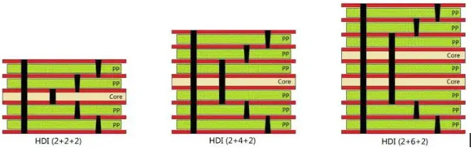
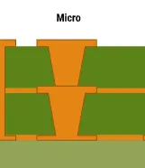
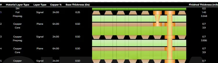
The root cause is not a designer error; it is the physics of multiple press cycles. Each time we laminate a new dielectric and copper foil, the panel expands and contracts. Even with good process control the residual stress and resin flow shift the already-drilled microvias relative to the next layer's pads. On a 1+N+1 construction the shift is usually manageable. On 2+N+2 or 3+N+3 the shifts stack. If the original design used a 50 µm annular ring on a 100 µm microvia, that ring is gone after the second lamination. From a fabrication standpoint this becomes sensitive because the laser drill cannot "see" the final registered position; it only sees the current layer. CAM therefore has to pre-compensate or force a larger pad so the via still lands inside copper after all movements have occurred.
Copper balance is the second driver. HDI outer layers often carry dense BGA or fine-pitch routing on one side and almost empty areas on the other. During plating the current density difference creates thickness variation of 8–12 µm across the panel. When the design already sits at minimum trace width, that thickness variation changes etch undercut and can open the trace or leave residual copper that shorts adjacent features. We flag these density maps during CAM review and either add thieving copper or ask for a layout redistribution.
What fails on the line when the changes are ignored
If the job proceeds without the CAM adjustments, the first failure mode is microvia open or intermittent contact. The laser drills the via correctly relative to the current layer, but after final registration the via sits on the edge of the capture pad or completely misses it. Electrical test catches some of these; the ones that pass test still fail after thermal cycling or reflow because the residual copper connection is too thin. Yield drops of 15–25 % on complex HDI panels are common when this is left uncontrolled.
The second failure is solder-mask registration shift relative to the fine-pitch pads. Sequential builds leave the outer layers with higher topography. Standard mask alignment tolerances of ±50 µm become insufficient; the mask either covers the pad or leaves an excessive opening that causes solder bridging at assembly. Scrap and rework then cascade into delayed shipments and extra ECN cycles.
How CAM and process engineering actually compensate
Most factories handle this by a fixed compensation matrix inside the CAM software. For laser microvias we enlarge the capture pad by 25–40 µm per sequential layer beyond the first. We also apply a global etch compensation of 10–15 µm per side on outer fine-line layers once the final copper thickness after plating is known. Panel copper balance is checked with a density map; any zone below 20 % copper gets thieving added automatically unless the customer has already filled the area.
When the design still cannot meet the process window after these adjustments, the CAM engineer does not simply reject the file. We open an engineering confirmation loop. The customer receives a marked-up Gerber set showing the exact locations that exceed capability, the proposed pad enlargement or via relocation, and the impact on impedance or BGA routing. Only after the customer signs the revised data do we release the job to laser drill. This single step cuts the later ECN rate dramatically because the change is locked before any material is cut.
Process parameters are also locked at this stage. Laser energy, pulse count, and plating current density are set according to the final stack and copper thickness that CAM has already validated. If the design later requires a change, the entire parameter set has to be re-qualified, which is why we push hard for the confirmation to happen once and only once.
When the factory can relax the rules without killing yield
Exceptions exist. Prototype runs of fewer than 20 panels can run with tighter annular rings if the customer accepts the risk of lower yield and signs a deviation form. Single-lamination 1+N+1 constructions with only one laser step also allow smaller capture pads because the registration stack is limited. When the design uses only through-vias on the outer layers and microvias only on the inner sequential cores, the outer-layer registration tolerance can be relaxed. In all of these cases the trade-off is explicit: higher scrap risk or longer cycle time versus keeping the original layout.
The practical way to reduce HDI CAM review changes and the subsequent ECN cycle is to treat the fab's process window as a design constraint from day one. Share the intended stack-up and the target microvia size with the CAM team before the layout is frozen. Most of the repeated modifications we see come from designs that were completed without that early check. Once the data is locked and the engineering confirmation is signed, further changes become expensive for both sides. Keeping the first CAM review clean is still the cheapest path through production.