In production we treat FR4 PCB barrel cracking as a reliability issue that is managed first at the plating and material stage. CAM engineers check the aspect ratio and copper thickness callout on every multilayer stack-up. For boards that will see multiple reflows or thermal cycling we hold a minimum average copper thickness of 25 µm in the barrel wall and push the plating process to deliver consistent coverage from the knee to the mid-barrel. High-Tg FR4 is preferred when the customer specification allows it, and we flag any design that combines high aspect ratio holes with thin copper or standard Tg material.
What we typically see on the CAM side is that designers request 1 oz finished copper on the surface while the barrel ends up with far less after etching and surface finish. We adjust the plating time and current density to bring the hole wall up to the target before the outer layer is etched. If the design cannot support that thickness we return a DFM note requesting either larger finished hole size or a reduction in layer count or aspect ratio.
CTE mismatch that puts the copper barrel under tension every time the board is heated
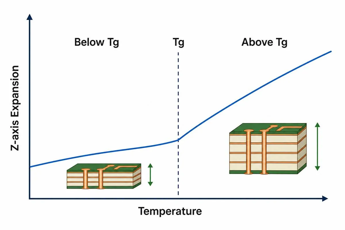
The main driver of FR4 PCB barrel cracking is the large difference in coefficient of thermal expansion between the copper plating and the surrounding FR4 laminate in the Z-direction. Copper expands at roughly 17 ppm/°C. Below Tg the FR4 resin/glass system is typically 40–60 ppm/°C; once the temperature exceeds Tg the resin expansion climbs rapidly, often exceeding 200 ppm/°C. During reflow, wave soldering or thermal cycling the board thickness grows more than the copper barrel can stretch. The resulting tensile stress concentrates at the knee of the hole and at any thin or voided areas in the plating.
In production this stress is unavoidable because every multilayer panel must go through lamination, solder mask cure, and at least one soldering cycle. The higher the aspect ratio, the longer the unsupported copper cylinder and the greater the strain. Residual stress left from drilling, desmear or plating adds to the thermal load. When the copper is thinner than about 20 µm the fatigue life drops sharply; cracks start after only a few thermal excursions.
What happens on the line and in the field when barrel cracks are left uncontrolled
If the copper thickness or material selection is not controlled, the board often passes bare-board electrical test because the crack has not yet fully separated the plating. After assembly the first reflow or thermal shock test opens the connection. In high-volume production this shows up as intermittent opens during ICT or functional test, or as early field returns once the product experiences temperature swings. Scrap rates climb when thermal cycling is part of the customer qualification; entire lots can be rejected after a failed IST or thermal shock sample. Rework is rarely practical once the crack is present, so the panels are written off and the shipment is delayed while a new lot is run with corrected plating parameters.
From a fabrication standpoint the problem becomes expensive because the defect is latent. Surface inspection and AOI do not catch it. Only cross-section or thermal stress testing reveals the crack, and by then the material and process costs are already sunk.
Plating thickness, material choice and process controls used to keep the barrel intact
Most factories handle FR4 PCB barrel cracking by enforcing a minimum average copper thickness of 25 µm in the hole wall for multilayer boards destined for multiple thermal cycles. We measure this on cross-section coupons taken from every production lot; the target is usually 25–30 µm with no local area below 20 µm. Pulse plating or high-throw chemistry is used on high-aspect-ratio panels to improve distribution. CAM also checks the finished hole size against the drill size so that the plating window is realistic; we will not accept a 0.25 mm finished hole on a 1.6 mm thick 8-layer board if the plating capability cannot guarantee the thickness.
Material selection is the second lever. High-Tg FR4 (Tg ≥ 170 °C) keeps the resin expansion lower through the soldering temperature range and reduces the peak strain on the copper. When the customer specification is open we recommend the higher Tg grade. Desmear and etchback parameters are kept tight so that the copper bonds cleanly to the glass and resin; poor adhesion creates another initiation site for cracks.
On the process side we control the cool-down rate after lamination and avoid rapid thermal shock during HASL or reflow simulation. For higher reliability builds we run sample thermal cycling or IST as part of the lot release. These steps add cost, but they catch the problem before the boards leave the factory rather than after assembly.
When thinner copper or standard Tg material is accepted without forcing a redesign
We relax the 25 µm rule for simple 4-layer boards with large holes (aspect ratio ≤ 6:1) that will see only one or two soldering operations and are intended for consumer or commercial applications with limited temperature range. In those cases 18–20 µm average copper is often accepted if the customer acknowledges the reduced fatigue life. Standard Tg material is likewise accepted when the end-use environment stays well below Tg and the thermal cycle count is low. The trade-off is clear: lower material and plating cost against a higher risk of latent opens if the product later sees more thermal stress than expected. For automotive, industrial or any high-reliability application we do not relax either the thickness or the Tg requirement.