In production we calculate the required plating thickness from the base copper foil weight and then lock the electroplating parameters before the panel ever hits the plating line. CAM engineers open the stack-up data, subtract the finished copper target from the starting foil thickness, and feed that delta into the plating time and current-density recipe. For a standard 1 oz FR4 board aiming at 35 µm finished outer copper we normally plate 20–25 µm; when the base foil is already 2 oz we drop the plating deposit to 10–15 µm and raise the current density slightly to keep the total within tolerance. That single calculation is the first gate that protects FR4 PCB plating thickness consistency.
Where base copper thickness starts to limit hole-wall coverage
The problem shows up as soon as the aspect ratio climbs above 8:1. Thicker base copper on the outer layers raises the surface conductivity, so the plating current prefers the surface over the hole wall. Inside a 0.3 mm hole drilled in 1.6 mm FR4 the current density at the center of the barrel can fall 30–40 % compared with the surface when the foil is 2 oz instead of 1 oz. That is pure geometry and conductivity: the thicker copper plane acts like a low-resistance path that steals current from the high-aspect-ratio feature. We see the same effect on internal layers when the buried vias sit under heavy copper planes. Material behavior of the FR4 itself does not change, but the copper distribution on the panel forces the plating bath to work against a non-uniform field.
Panelization makes it worse. When a large copper area sits next to a sparse via field the local current density swings even more. Most factories run a fixed rectifier set-point for the whole panel; once the copper thickness difference exceeds roughly 1 oz the rectifier cannot compensate and the thin spots appear first in the hole centers.
What the plating line actually delivers when copper thickness is left uncontrolled
If we ignore the base-copper effect and run the same plating recipe for every board, the hole-wall copper drops below 18 µm in the critical zone. That is the point where thermal-cycle reliability starts to fail. In practice we measure 12–15 µm on the barrel center while the surface is already at 40 µm. The thin wall cracks under reflow or thermal shock, the via opens, and the board is scrap. Yield loss on a 2 oz outer-layer FR4 panel can reach 8–12 % just from this mechanism when no compensation is applied.
Uneven plating also shows up as dog-bone copper at the hole knee. Excess copper builds at the surface entrance while the middle stays thin. Later, when the solder mask is applied, the thick knee can create mask tenting failures or solder bridges during assembly. Rework is almost never economical; the panel is usually scrapped and the order is delayed by one full plating cycle plus micro-section verification.
How we adjust current density and panel layout to keep FR4 PCB copper thickness plating consistent
Most factories solve it in three places: CAM compensation, rectifier programming, and panel design. First the CAM engineer runs a copper-balance check. If the outer-layer copper coverage differs by more than 15 % across the panel we insert plating thieves or dummy copper pads in the sparse areas. That equalizes the surface current density before the panel reaches the bath.
Next we calculate the required average current density. For standard FR4 we stay between 15–25 ASF. When the base foil is 2 oz or heavier we raise the surface current density 10–15 % and shorten the plating time so the total deposit still meets the finished copper target. Pulse plating is used on thick-copper jobs because the reverse pulse removes the excess at the surface and forces more copper into the hole. Typical pulse parameters are 20 ms forward / 2 ms reverse at 30–40 ASF peak.
On the plating line itself the operator measures the solution copper concentration and temperature every two hours; a 5 °C rise or a 2 g/L drop in copper ions is enough to shift the deposit thickness by 3–4 µm. We also run a test coupon on every panel that contains a range of hole sizes and copper densities. After plating the coupon is micro-sectioned and the wall thickness is recorded. If any hole falls outside the 20–25 µm process window the entire panel is stripped and re-plated with adjusted parameters.
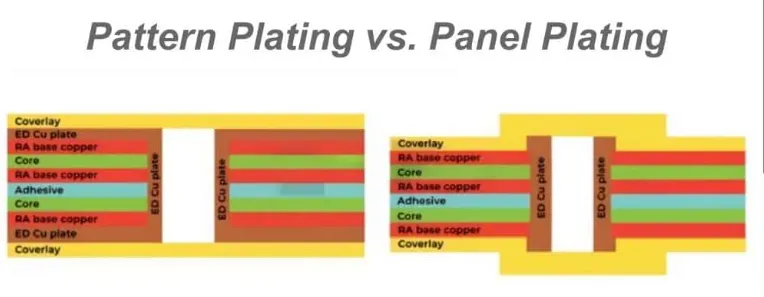
For boards that specify 3 oz or 4 oz finished copper we switch to a two-step plating process: first a thin flash to cover the hole wall, then a high-current build-up. This keeps the FR4 PCB plating thickness under control even when the starting foil is already heavy.
When we can relax the plating thickness window
Exceptions are limited. On prototypes with aspect ratios below 6:1 and no high-reliability requirement we accept a finished hole-wall minimum of 15 µm instead of 20 µm. The same relaxation applies to large-hole power boards where the current density is naturally more uniform. Trade-off is clear: lower process cost and shorter plating time, but the customer must accept reduced thermal-cycle life. For production volumes or IPC Class 3 boards the full compensation rules stay in force; we do not open the window just because the base copper is thick.
In short, FR4 PCB copper thickness plating is managed by calculating the deposit from the actual foil weight, balancing the panel copper, and locking the current-density recipe before the first ampere is applied. Ignore any of those steps and the hole wall is the first place the process fails.