










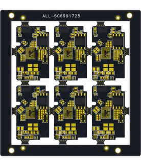
PCB Specifications
| Parameter | Value | Parameter | Value |
|---|---|---|---|
| PCB Type | HDI PCB | Quantity | 30 pcs |
| Layers | 6 Layers | Board Type | Panel PCB |
| Dimensions | 23.7 x 14.4 mm | Copper Weight | 1oz |
| Thickness | 0.6 mm | Min Track / Spacing | 4/4mil |
| Surface Finish | ENIG (Immersion Gold) | Min Hole Size | 0.1mm |
| Solder Mask | Black | Silkscreen | White |
| HDI Structure | 1 | Blind/Buried Vias | Yes |
Manufacturing Timeline
Logistics Information
Key Manufacturing Processes
Manufacturing Summary
These 6-layer High-Density Interconnect PCBs were manufactured in panel form with a production quantity of 30. Measuring 23.7 × 14.4 mm and only 0.6 mm thick, the boards incorporated a 1-step HDI structure with 0.1 mm laser-drilled blind vias. The tight 4/4 mil minimum track and spacing on this thin substrate required precise trace width compensation during inner layer imaging and etching to maintain design intent.
Sequential lamination was used to integrate the microvias reliably, followed by via filling and plating. Stackup impedance engineering guided the entire build, with TDR impedance testing performed to verify all controlled lines. Black soldermask, white silkscreen, and immersion gold ENIG surface finish completed the panels while ensuring good solderability on the dense layout.
Electrical testing confirmed full continuity and isolation across the batch. This impedance controlled HDI PCB order was completed in 15.3 days, delivering consistent results that matched the tight geometry, thin profile, and blind via requirements from start to finish.
Explore More PCB Manufacturing Resources
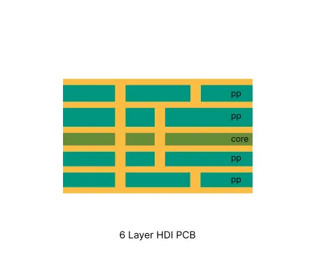
6 Layer HDI PCB Manufacturing Insights
Discover how AIVON manufactures 6 Layer HDI PCBs, including advanced microvia technology, multilayer interconnection control, sequential lamination processes, manufacturing challenges, and real production experience from customer orders.
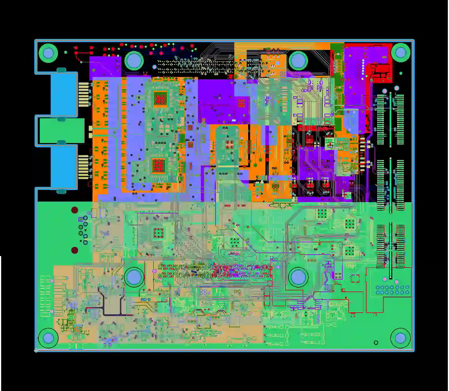
Multilayer HDI PCB Common Engineering Queries in Manufacturing
Multilayer HDI PCBs frequently trigger CAM EQs on microvia spacing, via-in-pad plugging, stack-up, and impedance. Learn real root causes and design rules that raise first-pass yield.
Real Production Records
| Order ID | PCB Type | Layers | Dimensions | Solder Mask | Surface Finish | Quantity | Action |
|---|---|---|---|---|---|---|---|
| HDI-20260729-036 | HDI PCB | 8 | 97 x 93.4 | Black | ENIG (Immersion Gold) | 100 | View detail |
| HDI-20260720-0001 | HDI PCB | 8 | 188 x 100 | Matte Black | ENIG (Immersion Gold) | 125 | View detail |
| HDI-20260718-0002 | HDI PCB | 4 | 37 x 26.6 | Green | ENIG (Immersion Gold) | 20 | View detail |


