










PCB Specifications
| Parameter | Value | Parameter | Value |
|---|---|---|---|
| PCB Type | HDI PCB | Quantity | 5 pcs |
| Layers | 8 Layers | Board Type | Panel PCB |
| Dimensions | 141 x 194 mm | Copper Weight | 1oz |
| Thickness | 1.6 mm | Min Track / Spacing | 3/3mil |
| Surface Finish | ENIG (Immersion Gold) | Min Hole Size | 0.15mm |
| Solder Mask | Matte Black | Silkscreen | White |
| HDI Structure | 3 | Blind/Buried Vias | No |
Manufacturing Timeline
Logistics Information
Key Manufacturing Processes
Manufacturing Summary
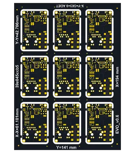
This 8-layer HDI PCB measured 141 × 194 mm with 1.6 mm thickness and used a 3-step structure for the high-density interconnect. Built in panel format for a quantity of 5 pieces, the design incorporated 1 oz copper, tight 3/3 mil line/space geometry, 0.15 mm minimum holes, matte black solder mask, and white silkscreen finished with ENIG. Process edges received copper pour to improve current balance across the panel.
DFM review identified several critical points. The supplied stackup followed a conventional 8-layer configuration that could not accommodate the blind via requirements, necessitating a revised press sequence. Fifty-ohm impedance traces lacked corresponding line-width data, requiring clarification against reference layers. Layer ordering was undefined in the source files and was established from the available Gerber set. Copper balancing on process edges was confirmed to reduce thermal and current imbalance during plating and assembly.
The revised stackup and impedance references were approved prior to release. Production proceeded with the adjusted lamination sequence and confirmed layer order, delivering consistent registration and plating across the fine-feature HDI structure. Full electrical testing verified performance, and the small-batch boards were completed to the specified ENIG and geometry requirements.
Explore More PCB Manufacturing Resources
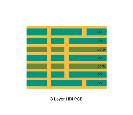
8 Layer HDI PCB Manufacturing Insights
Discover how AIVON manufactures 8 Layer HDI PCBs, including high-density interconnect structures, complex stackup management, microvia reliability, manufacturing challenges, and real production experience from customer orders.
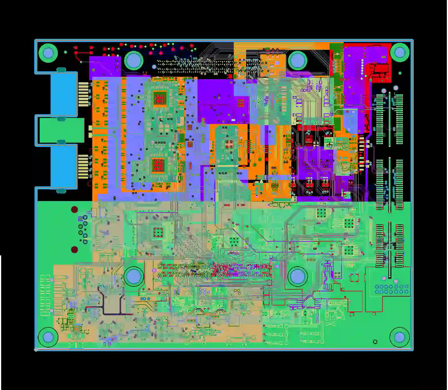
Multilayer HDI PCB Common Engineering Queries in Manufacturing
Multilayer HDI PCBs frequently trigger CAM EQs on microvia spacing, via-in-pad plugging, stack-up, and impedance. Learn real root causes and design rules that raise first-pass yield.
Real Production Records
| Order ID | PCB Type | Layers | Dimensions | Solder Mask | Surface Finish | Quantity | Action |
|---|---|---|---|---|---|---|---|
| HDI-20260729-036 | HDI PCB | 8 | 97 x 93.4 | Black | ENIG (Immersion Gold) | 100 | View detail |
| HDI-20260720-0001 | HDI PCB | 8 | 188 x 100 | Matte Black | ENIG (Immersion Gold) | 125 | View detail |
| HDI-20260718-0002 | HDI PCB | 4 | 37 x 26.6 | Green | ENIG (Immersion Gold) | 20 | View detail |


