










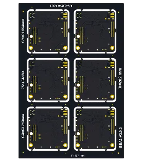
PCB Specifications
| Parameter | Value | Parameter | Value |
|---|---|---|---|
| PCB Type | HDI PCB | Quantity | 10 pcs |
| Layers | 8 Layers | Board Type | Panel PCB |
| Dimensions | 137 x 202 mm | Copper Weight | 1oz |
| Thickness | 1.6 mm | Min Track / Spacing | 3/3mil |
| Surface Finish | ENIG (Immersion Gold) | Min Hole Size | 0.1mm |
| Solder Mask | Matte Black | Silkscreen | White |
| HDI Structure | 3 | Blind/Buried Vias | No |
Manufacturing Timeline
Logistics Information
Key Manufacturing Processes
Manufacturing Summary
This 8-layer HDI PCB (137 × 202 mm, 1.6 mm thick) with 3-step structure was built as panels for 10 pieces. The design used tight 3/3 mil line/space, 0.1 mm minimum holes, 1 oz copper, matte black solder mask, and white silkscreen with ENIG finish. Multiple impedance requirements and precise via configurations defined the high-density interconnect stackup.
DFM analysis revealed conflicting impedance data and unclear layer/drill sequencing in the provided files. Blind vias exceeding 0.1 mm could not be laser drilled, requiring process adjustments. Inner layer references for 50 ohm lines were standardized, and pad enlargements were added on top layer for manufacturable copper clearance on specific holes. Production numbering placement and layer order were confirmed after stackup optimization.
Optimized lamination and impedance reference layers were implemented following customer approval. The HDI stackup and impedance control adjustments ensured electrical performance matched design intent. Production completed with full testing, delivering consistent boards that satisfied the fine-feature HDI requirements.
Explore More PCB Manufacturing Resources
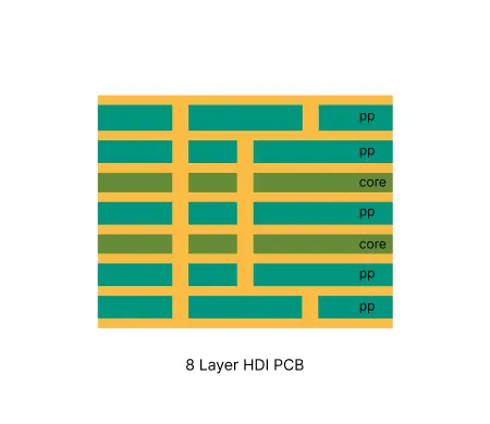
8 Layer HDI PCB Manufacturing Insights
Discover how AIVON manufactures 8 Layer HDI PCBs, including high-density interconnect structures, complex stackup management, microvia reliability, manufacturing challenges, and real production experience from customer orders.
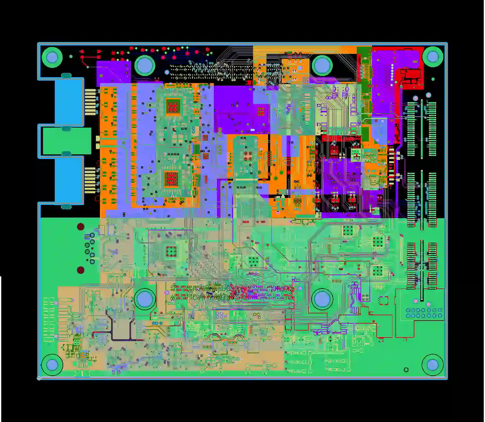
Multilayer HDI PCB Common Engineering Queries in Manufacturing
Multilayer HDI PCBs frequently trigger CAM EQs on microvia spacing, via-in-pad plugging, stack-up, and impedance. Learn real root causes and design rules that raise first-pass yield.
Real Production Records
| Order ID | PCB Type | Layers | Dimensions | Solder Mask | Surface Finish | Quantity | Action |
|---|---|---|---|---|---|---|---|
| HDI-20260729-036 | HDI PCB | 8 | 97 x 93.4 | Black | ENIG (Immersion Gold) | 100 | View detail |
| HDI-20260720-0001 | HDI PCB | 8 | 188 x 100 | Matte Black | ENIG (Immersion Gold) | 125 | View detail |
| HDI-20260718-0002 | HDI PCB | 4 | 37 x 26.6 | Green | ENIG (Immersion Gold) | 20 | View detail |


