










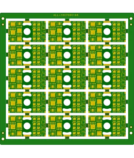
PCB Specifications
| Parameter | Value | Parameter | Value |
|---|---|---|---|
| PCB Type | HDI PCB | Quantity | 225 pcs |
| Layers | 16 Layers | Board Type | Panel PCB |
| Dimensions | 32 x 18 mm | Copper Weight | 1oz |
| Thickness | 2.2 mm | Min Track / Spacing | 6/6mil↑ |
| Surface Finish | ENIG (Immersion Gold) | Min Hole Size | 0.3mm↑ |
| Solder Mask | Green | Silkscreen | None |
| HDI Structure | 1 | Blind/Buried Vias | No |
Manufacturing Timeline
Logistics Information
Key Manufacturing Processes
Manufacturing Summary
This 16-layer HDI PCB order consisted of 225 panels fabricated using a custom stackup to achieve a 2.2 mm board thickness. The individual boards measure 32 x 18 mm with 1 oz copper weight and standard 6 mil minimum trace and spacing. Sequential lamination was performed in combination with laser microvia drilling and via filling to establish the necessary interconnections for the HDI structure.
Green soldermask and immersion gold ENIG surface finish were applied to meet the specified requirements, while omitting silkscreen printing. Multiple batch AOI inspections and end-of-line electrical testing ensured every panel maintained the required electrical performance and physical integrity across the full production run.
The manufacturing cycle spanned 17.2 days, providing sufficient time for precise layer alignment during high-pressure lamination and controlled plating operations. This execution delivered uniform quality for the entire quantity, supporting reliable field performance for these thicker HDI PCBs.
Explore More PCB Manufacturing Resources
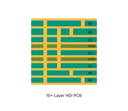
10+ Layer HDI PCB Manufacturing Insights
10+ layer HDI PCBs use sequential lamination and microvia technology to achieve high interconnect density in compact multilayer boards. Supports stacked or staggered microvias with laser-drilled structures. Compatible with high-Tg FR-4 and high-speed laminates.
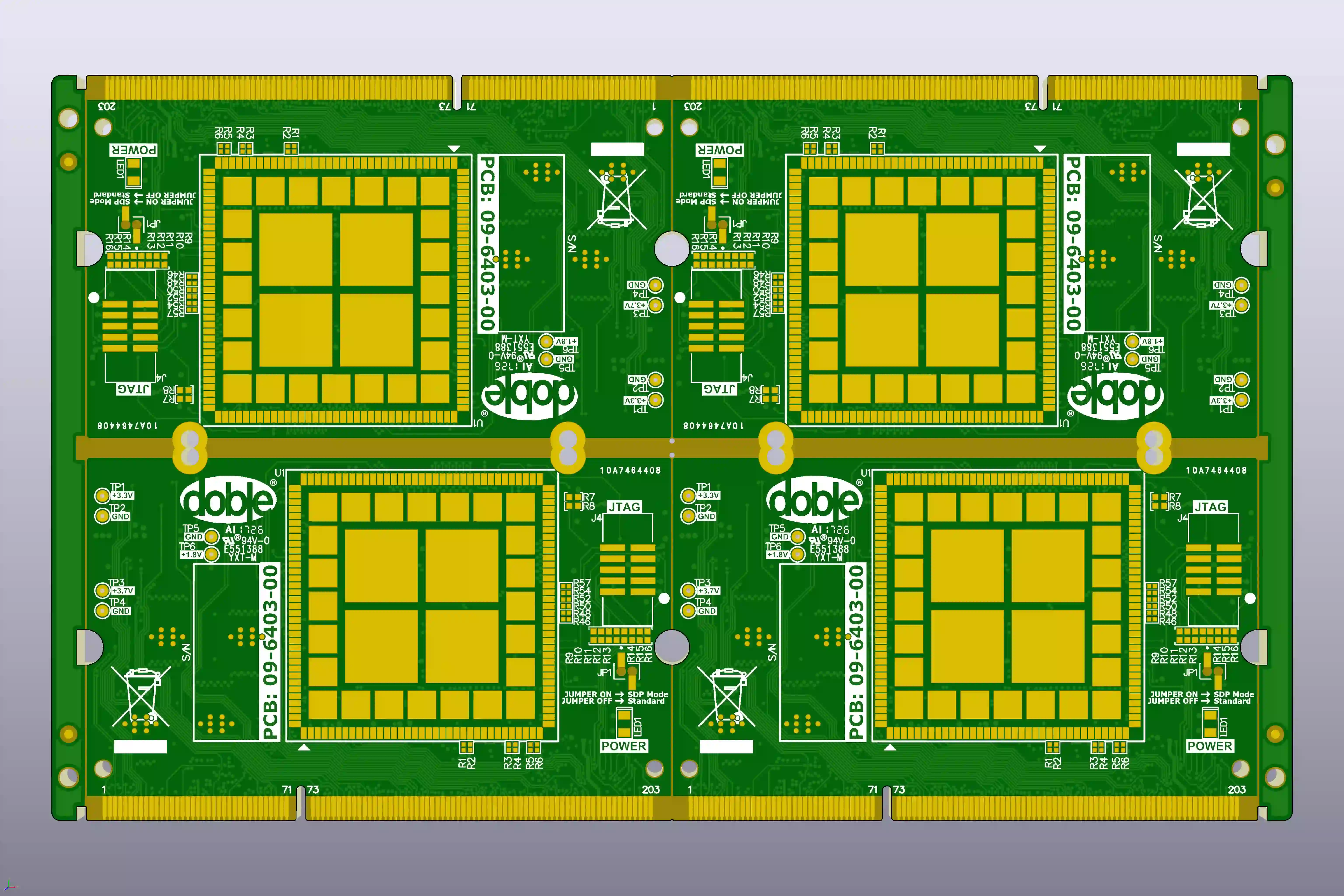
How to Resolve Gold Finger Bevel and Impedance EQs in 10-Layer PCBs
Real 10-layer FR-4 case study: how CAM engineers resolved gold finger bevel clearance, impedance mismatch, tight via spacing and plugging risks to prevent scrap and signal integrity failures.
Real Production Records
| Order ID | PCB Type | Layers | Dimensions | Solder Mask | Surface Finish | Quantity | Action |
|---|---|---|---|---|---|---|---|
| HDI-20260729-036 | HDI PCB | 8 | 97 x 93.4 | Black | ENIG (Immersion Gold) | 100 | View detail |
| HDI-20260720-0001 | HDI PCB | 8 | 188 x 100 | Matte Black | ENIG (Immersion Gold) | 125 | View detail |
| HDI-20260718-0002 | HDI PCB | 4 | 37 x 26.6 | Green | ENIG (Immersion Gold) | 20 | View detail |


