










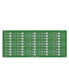
PCB Specifications
| Parameter | Value | Parameter | Value |
|---|---|---|---|
| PCB Type | HDI PCB | Quantity | 375 pcs |
| Layers | 16 Layers | Board Type | Panel PCB |
| Dimensions | 20.2 x 32.3 mm | Copper Weight | 1oz |
| Thickness | 2.2 mm | Min Track / Spacing | 4/4mil |
| Surface Finish | ENIG (Immersion Gold) | Min Hole Size | 0.1mm |
| Solder Mask | Green | Silkscreen | None |
Manufacturing Timeline
Logistics Information
Key Manufacturing Processes
Manufacturing Summary
This 16-layer HDI board measured 20.2 × 32.3 mm with mixed 2 oz / 1 oz copper and a 2.2 mm finished thickness using Shengyi S1000-2M TG170 material. Produced in a quantity of 375 pieces as 3×5 panels with 4 mm process edges on all sides, the design featured 4 mil line/space, 0.1 mm holes, blind vias, resin plugging, and ENIG surface finish. The high layer count and tight geometry on a relatively small panel presented significant stackup and plating challenges.
DFM review required multiple adjustments to the provided stackup. The original dielectric thicknesses were too thin to reliably achieve 2.2 mm finished board thickness without delamination risk using the minimum 0.11 mm 2 oz cores. Copper weight conflicts arose from the 4 mil geometry, where 2 oz outer layers would remove excessive copper bridges. Through-hole vias overlapping SMT pads risked voids without plugging. Final configuration used 1 oz on layers 1-2-3-14-15-16 and 2 oz on remaining layers to balance thickness and spacing requirements. Stamp hole panelization was adopted due to panel size constraints. Resin plugging reliability handling was implemented for vias on pads to prevent solder joint defects.
Production advanced after customer confirmation of the revised stackup and panel method. All boards passed 100% flying probe testing and met dimensional tolerances despite the high layer count and mixed copper configuration, supporting reliable performance for this volume order.
Explore More PCB Manufacturing Resources
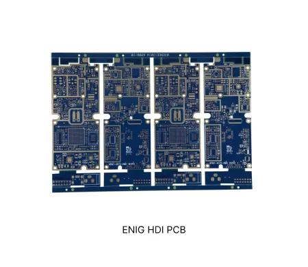
ENIG HDI PCB Manufacturing Insights
ENIG finished HDI PCBs require precise control of sequential lamination, laser drilling, copper plating, and electroless nickel immersion gold deposition to ensure via reliability and solderable surfaces.
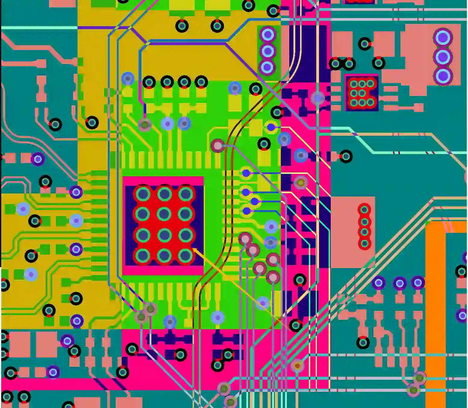
Common Engineering Issues in HDI PCB Manufacturing with Different Surface Finishes
This article provides senior engineering insights into HDI PCB manufacturing with different surface finishes such as ENIG and OSP. It covers common engineering queries including via-in-pad design, solder mask registration, microvia reliability, and surface finish compatibility, along with practical DFM solutions to improve fabrication yield.
Real Production Records
| Order ID | PCB Type | Layers | Dimensions | Solder Mask | Surface Finish | Quantity | Action |
|---|---|---|---|---|---|---|---|
| HDI-20260729-036 | HDI PCB | 8 | 97 x 93.4 | Black | ENIG (Immersion Gold) | 100 | View detail |
| HDI-20260720-0001 | HDI PCB | 8 | 188 x 100 | Matte Black | ENIG (Immersion Gold) | 125 | View detail |
| HDI-20260718-0002 | HDI PCB | 4 | 37 x 26.6 | Green | ENIG (Immersion Gold) | 20 | View detail |


