










PCB Antipads: Via Clearance Essentials for Multilayer PCB Reliability
What This Video Covers
While pads connect components and traces, antipads serve the equally important opposite function in modern multilayer PCBs. This video clearly explains what antipads are — clearance areas in copper planes (typically power or ground) around vias and through-holes that prevent unwanted electrical connections.
The content details how antipads allow a via to pass through a plane without shorting to it, while their size directly influences parasitic capacitance and overall signal integrity. In high-speed and controlled impedance designs, carefully sized antipads become critical for maintaining signal quality and reducing crosstalk.
Antipads are essential in 4-layer PCB, multilayer PCB, HDI PCB, and high-frequency PCB stack-ups. Proper antipad design supports better power distribution, cleaner return paths, and higher reliability across applications such as IoT devices, industrial control systems, automotive electronics, and aerospace PCB.
Understanding the balance between pads and antipads helps engineers avoid common manufacturing and performance issues early in the design phase.
Key Highlights
- Clearance Function: Antipads create deliberate gaps in power and ground planes so vias can pass through without making electrical contact.
- Signal Integrity Impact: Antipad size controls parasitic capacitance around high-speed vias, directly affecting impedance and signal quality.
- Design Balance: Pads connect components while antipads isolate them from planes — both are essential for functional, high-performance PCBs.
Clearance Design Principles for Vias in Copper Planes
In multilayer PCB construction, antipads function as deliberate non-copper zones surrounding vias and through-holes within power and ground planes. These clearance areas ensure that a via carrying a signal or other net does not form an unintended electrical connection to the plane copper during lamination, plating, or final assembly. Without properly sized antipads, even minor layer-to-layer misalignment can create direct shorts that render the board non-functional.
The geometry of an antipad directly influences the transition of a via through reference planes. In a typical 4-layer or 6-layer stack-up, the antipad diameter must exceed the via pad diameter plus the minimum clearance specified by the fabricator. This isolation supports clean layer transitions while preserving the integrity of the return path for high-speed signals. Real production data shows that inadequate clearance remains one of the top causes of electrical test failures in multilayer boards.
Designers must consider both the electrical and mechanical aspects of antipad placement. The clearance must accommodate drill wander during mechanical drilling and registration tolerances during sequential lamination. When these factors are ignored early in layout, the board may pass initial design rule checks but fail during fabrication or in the field under thermal or mechanical stress.
Balancing Antipad Size for Optimal Electrical Performance
Antipad dimensions directly govern parasitic capacitance between the via barrel and adjacent reference planes. Larger antipads reduce this capacitance, which helps maintain controlled impedance and lowers the risk of signal distortion or crosstalk in high-frequency circuits. However, excessively large clearances can fragment copper areas in power planes, increasing inductance and degrading power delivery network performance.
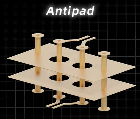
In high-speed digital and RF designs, engineers often perform 3D electromagnetic simulations to determine the optimal antipad diameter for target impedance. A via with an undersized antipad may exhibit higher capacitance, shifting impedance below specification and causing reflections visible in time-domain reflectometry measurements. Conversely, oversized antipads in dense designs can reduce available routing channels and affect thermal dissipation in power-intensive applications.
Practical manufacturing experience demonstrates that the ideal antipad size represents a compromise between electrical requirements and fabrication capabilities. Many fabricators recommend a minimum radial clearance of 0.15–0.25 mm beyond the via pad, depending on layer count and technology. Designers who treat antipad sizing as an afterthought frequently encounter impedance mismatches that require costly respins.
Pad vs Antipad Comparison
| Aspect | Pad | Antipad | Primary Function |
|---|---|---|---|
| Location | Component footprints and via lands | Copper planes surrounding vias | Provides isolation from plane copper |
| Manufacturing Risk if Undersized | Weak solder joint or insufficient annular ring | Via-to-plane short after plating or lamination | Controls parasitic capacitance and impedance |
| Effect on Signal Integrity | Minimal direct impact | Controls parasitic capacitance and impedance | Provides electrical connection |
| Typical Design Focus | Annular ring and solderability | Clearance margin accounting for registration tolerances | Provides isolation from plane copper |
Manufacturing Tolerances and DFM Rules for Antipads
Successful antipad implementation requires early collaboration with the PCB fabricator to incorporate their specific process capabilities. Layer registration accuracy in multilayer lamination typically ranges from ±0.05 mm to ±0.10 mm depending on board size and material. Drill positional tolerance for mechanical vias adds further variation. These cumulative tolerances must be added to the nominal clearance to prevent yield loss.
Common production issues arise when antipads are defined too tightly for the chosen stack-up. During plating, copper can bridge across an insufficient gap if the via is slightly off-center, creating latent shorts that pass initial electrical testing but fail under load or temperature cycling. In sequential build-up processes used for HDI boards, laser-drilled microvias demand even tighter control because the build-up dielectric thickness and alignment precision directly affect effective clearance.
Designers should load the fabricator's DFM rules into their CAD software before finalizing via placement. Adding fabrication notes that explicitly state minimum antipad clearance and reference the stack-up helps prevent misinterpretation. Post-design review of the copper pour around critical vias, combined with cross-section analysis of prototype boards, validates that the implemented clearance meets production reality rather than theoretical minimums.
Enhancing PCB Reliability Through Proper Antipad Implementation
Proper antipad design contributes to long-term reliability across demanding environments. In automotive electronics, where boards experience vibration, thermal cycling, and humidity, insufficient clearance can lead to intermittent shorts or dendritic growth over time. Industrial control systems similarly benefit from robust plane isolation that maintains clean return paths and reduces EMI susceptibility.
When antipads are correctly sized and documented, the resulting boards exhibit higher first-pass yield and fewer field returns. Fabricators report that designs incorporating conservative clearance margins aligned with their process capabilities consistently achieve better than 98% electrical test pass rates on complex multilayer jobs. This reliability advantage becomes especially valuable in applications requiring long product lifecycles or safety-critical operation.
Engineers should treat antipad definition as an integral part of stack-up planning rather than a post-layout adjustment. Reviewing impedance reports, power integrity simulations, and DFM feedback in a single design iteration cycle prevents late-stage changes that delay production. The cumulative effect of these disciplined practices is measurable improvement in both manufacturing yield and end-product performance.
FAQ
Q1: What is the difference between a pad and an antipad in PCB design?
A1: A pad provides copper for component connection or trace attachment. An antipad is the clearance area in a copper plane that prevents a via from shorting to that layer.
Q2: Why are antipads important in high-speed PCB designs?
A2: Antipad size controls parasitic capacitance between the via and reference planes, which impacts impedance control, signal integrity, and crosstalk in high-frequency applications.
Q3: How do antipads affect power and ground planes?
A3: Antipads ensure vias carrying signals or other nets do not unintentionally connect to power or ground planes, enabling clean layer transitions and proper power distribution.
Q4: What manufacturing tolerances must designers account for when specifying antipad sizes?
A4: Layer-to-layer registration, mechanical drill wander, and etching tolerances accumulate during multilayer fabrication. Typical registration accuracy ranges from ±0.05 mm to ±0.10 mm. Designers should add margin beyond the fabricator’s minimum clearance and verify the final stack-up with the manufacturer to avoid via-to-plane shorts after plating.
Q5: How can improper antipad design lead to manufacturing defects?
A5: Undersized antipads combined with registration error allow plated copper to bridge to the plane, causing electrical shorts and scrap. Oversized antipads may reduce power plane effectiveness or create etching difficulties in dense areas. Both conditions often require costly rework or respins when discovered after lamination.
Everyone knows a PCB has pads.But did you know PCBs also have antipads?
An antipad is a clearance area in a copper plane around a via or hole.
It prevents the via from connecting to that copper layer.
Without an antipad, a via passing through a power or ground plane would automatically connect to it.
Antipads create a gap so the via can pass through the layer without making electrical contact.
Antipads also affect signal integrity.
The size of the clearance changes the parasitic capacitance between the via and the plane. That's why in high-speed designs, antipad size is carefully controlled.
You'll find antipads mostly in: power and ground planes;high-speed signal vias and controlled impedance designs.
Pads connect things.Antipads make sure they don't.
And both are essential to a working PCB.





