










HDI Slot Design: Plated and Non-Plated PCB Slot Holes for Reliable HDI Boards
What This Video Covers
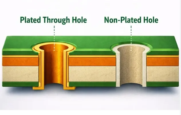
PCB slot holes — elongated openings created by drilling followed by routing — and why they are used instead of standard round holes in many designs. Slot holes serve both electrical and mechanical purposes, with plated slots providing electrical connections and non-plated slots offering clearance, fitment, or increased isolation.
Plated slots present unique manufacturing challenges during PCB fabrication: narrow or long slots can lead to uneven copper plating, weakening the barrel in the middle. Non-plated slots require careful layout to maintain proper copper clearance and creepage distance. Key design considerations include tool size limits on minimum width, width-to-thickness ratio for reliable plating, pad support with rounded ends for plated slots, and sufficient isolation for non-plated ones.
Proper implementation improves mechanical stress resistance and reliability in dense multilayer boards and HDI PCB designs. The video provides practical guidelines to avoid common defects during PCB prototype and PCB mass production.
These details are critical for high-reliability applications such as automotive PCB, medical devices PCB, and aerospace PCB, helping OEM teams reduce production issues when ordering PCB assembly.
Key Highlights
- PCB slot holes are created by drilling then routing and come in plated (electrical) and non-plated (mechanical/clearance) types.
- Plated slots require pad support and rounded ends to ensure even copper plating and prevent weak spots in the barrel.
- Design rules focus on minimum width limits, aspect ratio, and copper clearance to maintain reliability and avoid manufacturing defects.
HDI Slot Manufacturing Challenges in Plated and Non-Plated PCB Holes
In PCB fabrication, slot holes are typically formed by a combination of mechanical drilling for the ends and routing for the elongated section. This process introduces specific difficulties compared to standard round vias. For plated slots, the primary issue is achieving uniform copper deposition along the entire barrel length. Electrolytic plating solutions flow less effectively in narrow, elongated openings, often resulting in thinner copper at the center and thicker deposits near the ends. This non-uniformity reduces the slot's current-carrying capacity and mechanical strength.
Non-plated slots avoid plating but demand precise routing to prevent burrs or resin smear that can affect subsequent assembly steps. Tool deflection during routing of long slots can also cause dimensional inaccuracies, leading to fitment problems with connectors or mechanical fasteners. In multilayer boards, misalignment between layers exacerbates these issues, potentially causing short circuits or insufficient isolation.
Production data from high-volume runs shows that slots narrower than 0.8 mm or with aspect ratios exceeding 5:1 frequently trigger quality alerts. Fabricators must adjust plating parameters, such as current density and agitation, which increases cycle time and cost. Designers who ignore these realities often face higher scrap rates and delayed time-to-market.
HDI Slot Design Rules: Dimensions, Clearance, and PCB Slot Standards
Effective DFM for PCB slot holes starts with minimum width constraints dictated by available routing tools. Standard minimum slot widths typically range from 0.5 mm to 1.0 mm depending on board thickness and fabricator capability. Rounded ends are mandatory for plated slots to eliminate stress concentrations and improve plating distribution.
Pad support around plated slots should extend at least 0.15 mm beyond the slot outline, with thermal reliefs carefully balanced to avoid solder wicking issues during assembly. For non-plated slots used for creepage enhancement, maintain copper-to-edge clearances of at least 0.3 mm (or per voltage requirements) to prevent arcing in high-voltage applications.
Aspect ratio guidelines recommend keeping slot length-to-width below 8:1 for reliable plating in standard processes. In HDI designs, laser-drilled microslots require even stricter controls. Collaboration with the manufacturer during the design review phase allows optimization of these parameters before tooling begins, significantly reducing revision cycles.
Plated vs Non-Plated Holes in PCB: Slot Structure and Manufacturing Differences
PCB slot holes find extensive use in connectors, heat sinks, and component mounting where round holes would limit alignment flexibility or current capacity. In automotive electronics, elongated slots accommodate thermal expansion differences between modules and the board, reducing solder joint stress during temperature cycling. Medical device PCBs utilize non-plated slots to increase isolation distances in patient-contact circuits while maintaining compact layouts.
Aerospace applications benefit from the enhanced mechanical locking provided by slotted mounting points, which resist vibration-induced loosening better than circular holes. In power electronics, wide plated slots serve as high-current bus connections, distributing heat and current more effectively than multiple round vias.
When properly designed, slot holes contribute to overall board robustness, lowering field failure rates in harsh environments. Real-world case studies demonstrate up to 30% improvement in mechanical retention force and better signal integrity in dense layouts when DFM principles are followed from the outset.
| Parameter | Plated Slot Holes | Non-Plated Slot Holes |
|---|---|---|
| Primary Purpose | Electrical connection & mechanical | Mechanical fitment & isolation |
| Minimum Width | 0.6–0.8 mm typical | 0.5 mm typical |
| Aspect Ratio Limit | ≤ 5:1 recommended | ≤ 10:1 possible |
| End Shape | Rounded mandatory | Rounded preferred |
| Copper Clearance | Standard annular ring | ≥ 0.3 mm to edge |
| Common Risk | Uneven plating in center | Insufficient creepage distance |
Common Failure Modes and Prevention Strategies
Uneven plating remains the most frequent defect in plated PCB slot holes, manifesting as barrel cracks after thermal stress testing. Prevention involves limiting slot length, incorporating multiple plating baths with intermediate rinses, and verifying copper thickness via microsection analysis on first articles.
Routing-induced delamination or burr formation in non-plated slots can cause assembly rejects. Using sharp, properly maintained router bits and optimizing feed rates mitigates this. Another common issue is inadequate clearance around non-plated slots leading to voltage breakdown; always calculate creepage according to IPC-2221 standards for the working voltage.
Early design reviews with the chosen fabricator, combined with comprehensive DFM checks, catch these problems before production. Prototype validation using accelerated life testing further confirms slot hole reliability under intended operating conditions.
FAQ
Q1: What is the difference between plated and non-plated PCB slot holes?
A1: Plated slot holes carry electrical signals with copper in the barrel, while non-plated slots are used for mechanical fit, alignment, or increasing creepage distance and isolation.
Q2: Why do long or narrow PCB slot holes cause manufacturing problems?
A2: Long or narrow slots lead to uneven plating in plated holes, resulting in weak copper deposits in the center, and can compromise isolation if copper is placed too close in non-plated designs.
Q3: What design rules should be followed for PCB slot holes?
A3: Use rounded ends and pad support for plated slots, respect tool size minimum width, maintain proper aspect ratio, and ensure adequate copper clearance for non-plated slots.
Q4: How do PCB slot holes improve reliability in automotive and medical applications?
A4: Slot holes accommodate thermal expansion, provide stronger mechanical retention under vibration, and allow optimized creepage distances. Following DFM guidelines prevents plating defects and ensures consistent performance across temperature and humidity extremes typical in these industries.
Q5: Can slot holes be used in HDI PCBs, and what special considerations apply?
A5: Yes, but HDI slot holes require laser or plasma processing with tighter tolerances. Designers must verify fabricator capabilities for microslot plating uniformity and consider stacked microvia transitions near slots to maintain signal integrity.
Why do some PCB holes look like tiny slots instead of circles?
Those are slot holes.
A slot is made by drilling first, then routing.
Some are plated to carry electrical connections, while others are non-plated for fit, clearance, or isolation.
For plated slots, the challenge is manufacturing.
If the slot is too narrow or too long, plating becomes uneven and weakens the copper in the middle.
For non-plated slots, the issue is layout.
Copper placed too close can reduce isolation.
What really matters is simple:
tool size limits the minimum width, the ratio between slot width and board thickness affects plating, and geometry affects stress.
In practice, plated slots need pad support and rounded ends.
Non-plated slots should stay clear of copper and help increase creepage distance.





