 00:54
00:54
PCB Plating
PCB plating is a critical process in the manufacturing of printed circuit boards, involving the deposition of metallic coatings onto the board's surface and vias to enhance conductivity, protect against corrosion, and ensure reliable solderability. This tag, PCB Plating, gathers a collection of in-depth articles that explore the various techniques, materials, and considerations essential for engineers, designers, and manufacturers working with electronics. Whether you are troubleshooting plating defects in a prototype or optimizing production for high-reliability applications, understanding these fundamentals can significantly impact the performance and longevity of your PCBs. Common plating methods include electroless nickel immersion gold (ENIG), hot air solder leveling (HASL), and immersion tin, each offering distinct advantages depending on factors like cost, environmental resistance, and compatibility with lead-free soldering. For instance, ENIG provides excellent surface planarity and oxidation resistance, making it ideal for fine-pitch components in consumer electronics and telecommunications. Practical insights from our articles cover best practices such as selecting the right plating thickness to minimize signal loss in high-frequency designs, or addressing common issues like black pad syndrome through proper process controls. By applying these strategies, you can reduce manufacturing defects, comply with industry standards like IPC-4552, and achieve better yields in assembly lines. For those seeking to deepen their knowledge, the resources under this tag offer detailed case studies and comparisons that can guide your decision-making in real-world scenarios. Reviewing these pieces will help you stay informed on emerging trends, such as eco-friendly plating alternatives that align with sustainability goals in electronics manufacturing.
Video Guide

Technical Articles

PTH Plated-Through-Hole Performance Metrics: The Hidden Lifeline of SMT Reliability
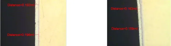
SMT Failure Case Study: Abnormal Plating on Fan Connector Pins After High-Temperature Wave Soldering
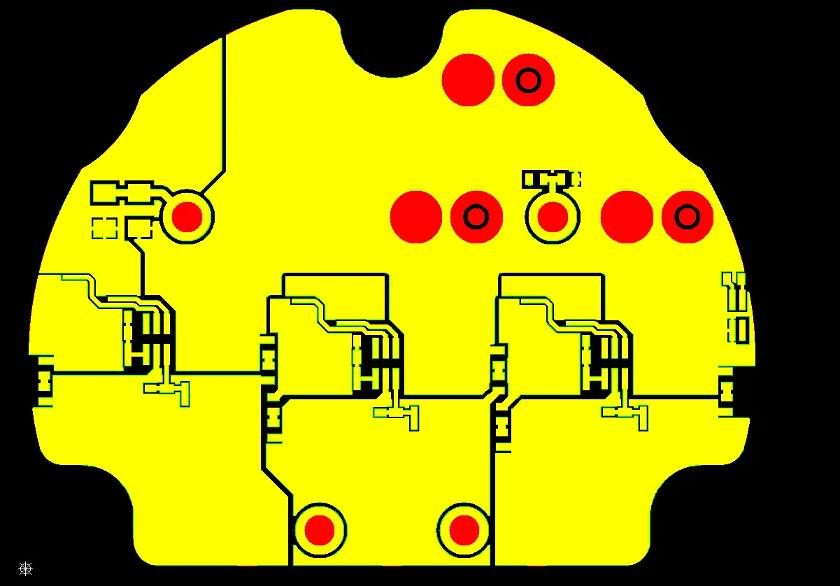
Why PCB CAM Must Verify PTH and NPTH Hole Definitions

Manufacturing Improvements to Prevent Lifting and Residual Shorts in PCB Gold-Finger Plating Leads
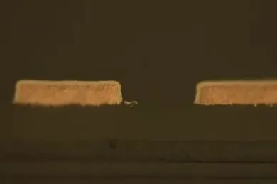
What Roles Does Palladium Play in PCB Manufacturing?

Why Identical Drill and Pad Sizes Risked Via Failures in a 6-Layer FR4 PCB

Press-Fit Interconnects for Electronics: Principles, Materials, Process, and Controls
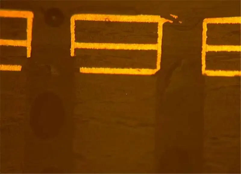
Analysis of PCB Inner-Layer Copper Voids and Hole Breaks: Causes and Corrective Measures
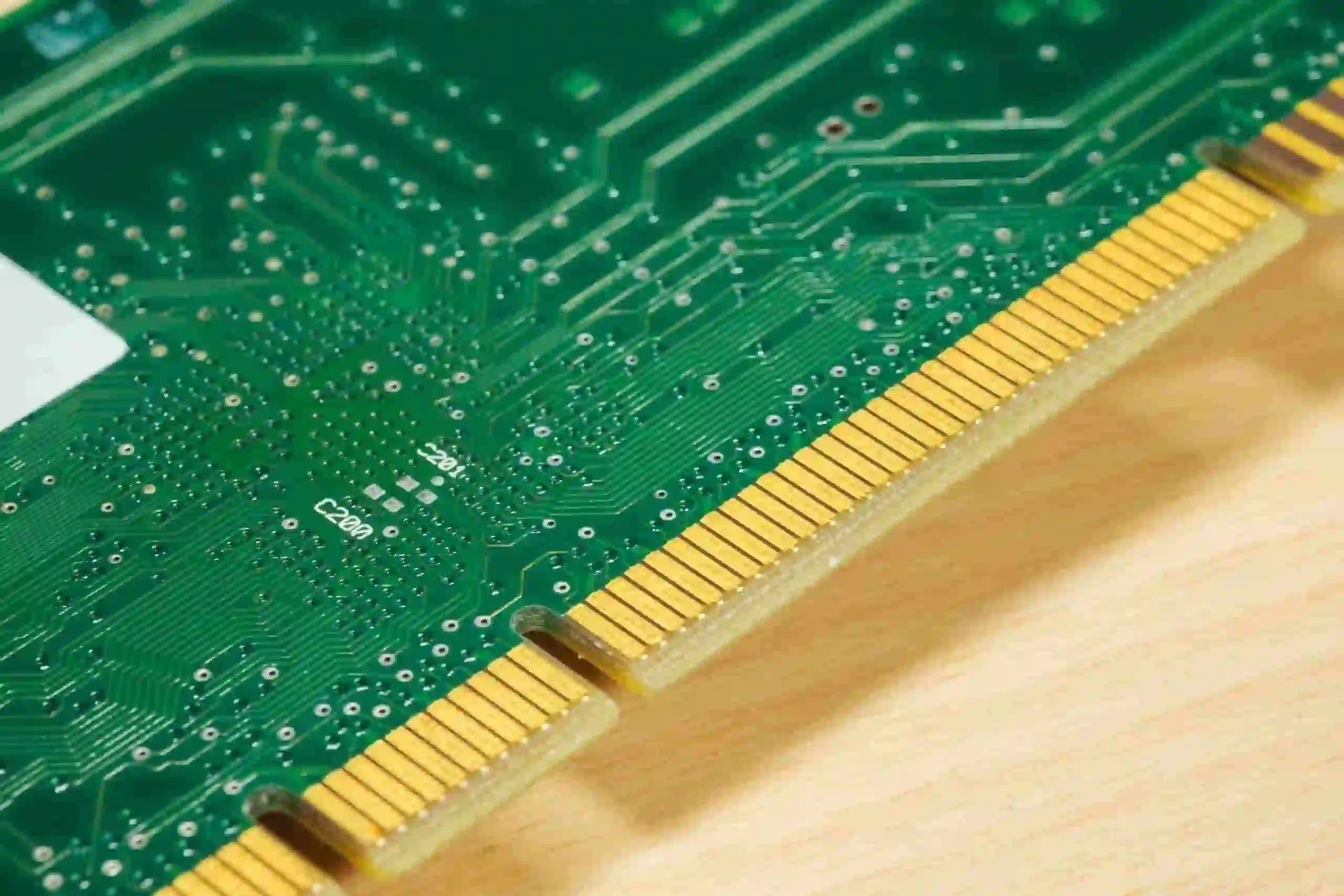
Resolving PCB Gold Finger Plating Problems: A Comprehensive Guide
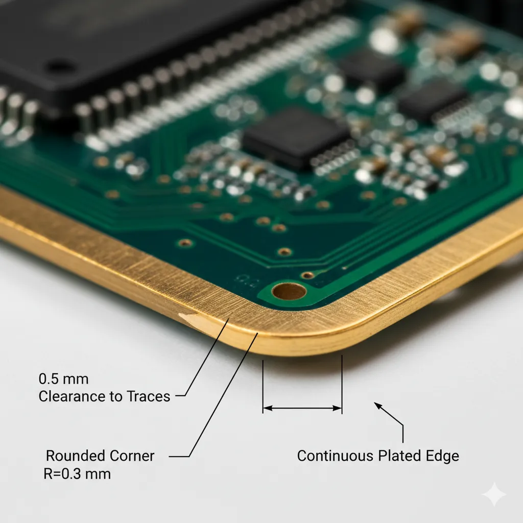
PCB Edge Plating Explained: A Guide for Electrical Engineers
How CAM Review Prevents Impedance Failures in 18-Layer PCBs
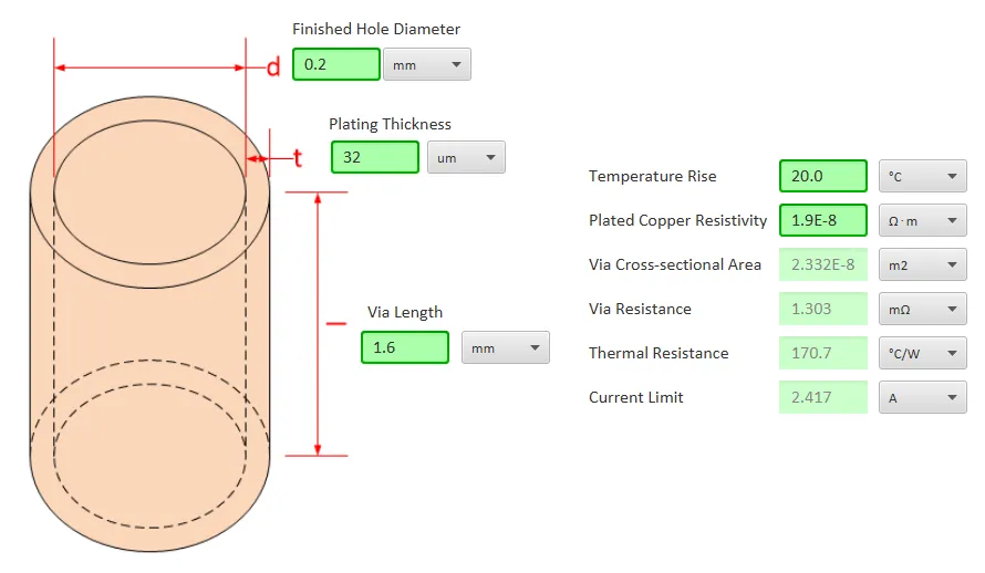
The Impact of PCB Aspect Ratio on Signal Integrity: A Deep Dive for High-Speed Designs
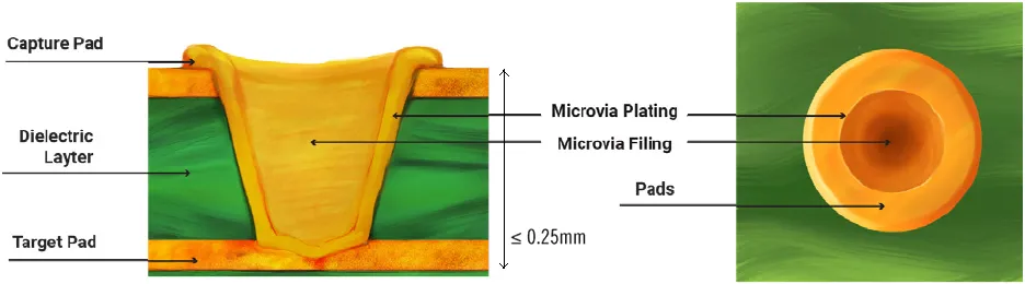
High Aspect Ratio PCBs: Challenges, Solutions, and Advanced Manufacturing Techniques
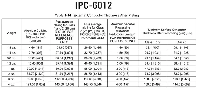
IPC 6012: A Detailed Examination of Hole/Via Plating Thickness Requirements
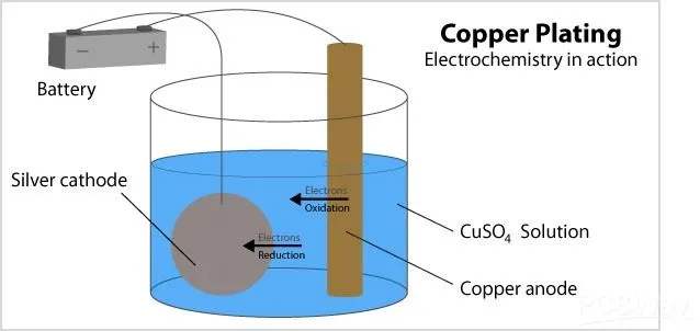
Electroless vs. Electrolytic Plating: Which Method is Right for Your PCB?
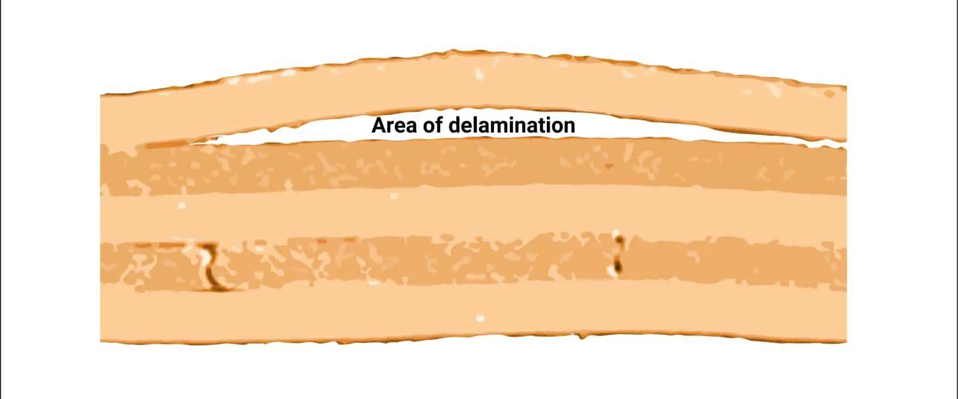
Overcoming PCB Manufacturing Challenges: Solutions for Common Defects and Production Issues
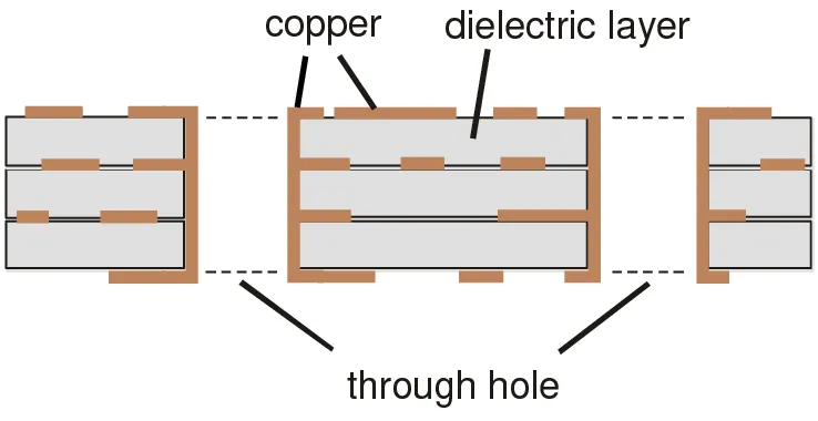
Copper Weight in PCB Manufacturing: Understanding Its Impact on Performance
Salt Spray Testing for Sheet Metal Corrosion Resistance: Standards Explained
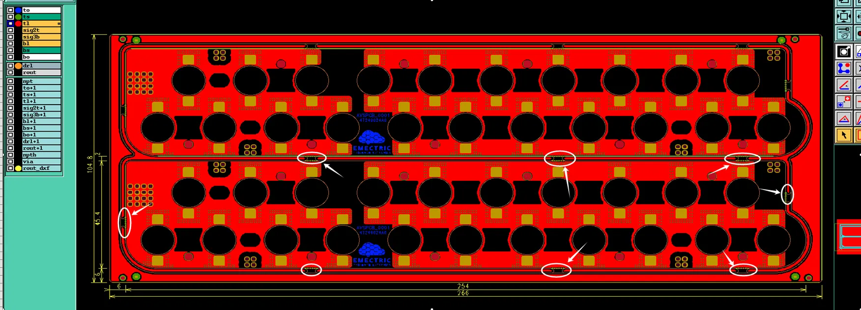
PCB Press-Fit Hole Design Rules for Heavy Copper Boards