










Positive vs. Negative PCB Processing: How Circuits Are Formed
What This Video Covers
This video explains how a finished copper circuit is created from a copper-clad panel using two factory routes: positive PCB processing and negative PCB processing. Both start with laminated photoresist. In the positive route, developed resist covers non-circuit areas, circuit copper is plated, tin is added as an etch resist, the film is stripped, unwanted copper is etched, and the tin is removed. In the negative route, resist covers the circuit itself, exposed copper is etched, and the film is stripped.
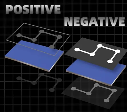
That split is not academic. Positive processing is the common method for outer-layer pattern plating, where plated through-holes and surface traces must grow together. Negative processing is the simpler, lower-cost path used on many inner layers of a 4 layer PCB, 6 layer PCB, or 8 layer PCB. The correct choice depends on stack-up, copper weight, minimum trace/space, and whether the layer must carry plated holes.
Engineers specifying HDI PCB layouts, FR4 PCB multilayer boards, or a PCB prototype should treat process selection as a DFM decision, not a drawing preference. The same netlist can be built either way; yield, etch factor, and plating thickness will not.
Key Highlights
- Positive processing opens the circuit areas after develop, plates copper then tin, strips resist, etches unused copper, and strips tin — the standard outer-layer pattern-plating sequence.
- Negative processing leaves resist on the circuit, etches the exposed copper, then strips resist — a shorter, more economical inner-layer print-and-etch route.
- Both routes can produce the same final circuit; the factory choice follows board structure (outer vs. inner, PTH requirement, copper weight) rather than the schematic.
How Positive PCB Processing Builds Outer-Layer Circuits
A copper-clad panel is cleaned and dry-film resist is laminated. After exposure and development, the resist remains over the non-circuit copper. Circuit areas — traces, pads, and the mouths of plated holes — are left open. Those openings are then electroplated with copper so surface traces and hole walls grow at the same time. A thin tin (or tin-lead) layer is plated on top of that copper. Tin is the real etch resist on this route; the dry film is only a plating mask.

The film is stripped, exposing the original foil in the non-circuit regions. Alkaline etch removes that foil. The tin cap is then stripped, leaving raised plated traces and plated through-holes. This SES sequence (strip–etch–strip after pattern plating) is why outer layers can carry current through the hole barrel and the surface trace as one conductor.
Factory risk is concentrated in plating distribution and etch undercut. Isolated fine traces plate faster than dense ground pours; without thieving or dummy copper, isolated nets can overplate while BGA neighborhoods starve. After etch, the plated trace often has an inverted-trapezoid cross-section: the top is slightly wider than the base because the tin cap shadows the sidewall. That geometry is acceptable for most signal layers, but it changes the finished width versus the artwork. CAM must apply an etch compensation so a 4 mil designed trace does not finish at 3.2 mil after etch.
Positive processing is also the reason outer-layer copper weight is not "just the foil." Finished outer copper is foil + plated copper. Specifying 1 oz finished copper on the outer layers of a 6 layer PCB usually means starting with thinner foil and plating up. If the stack-up note and the Gerber copper weight disagree, the shop will either over-etch or overplate. Resolve that in the fabrication notes before the panel is imaged.
How Negative PCB Processing Forms Inner-Layer Circuits
Inner layers usually do not need plated holes at the imaging step. The panel is still a copper-clad core. Resist is laminated, exposed, and developed so that the circuit itself stays covered. Uncovered copper is etched away. The resist is stripped. What remains is the etched inner-layer pattern — traces, clearances, and plane pours — at the original foil thickness.

That shorter DES sequence (develop–etch–strip) is cheaper and faster because it skips pattern plating and tin strip. It is the default for most inner signal layers and for many inner planes on FR4 PCB multilayer work. Planes are often drawn as negative artwork in CAD (clearances drawn, copper implied), but the factory still images them as a print-and-etch layer. Confusing "negative plane in the CAD tool" with "negative process in the factory" is a common CAM hold. If an inner layer shows only scattered pads and no pour, the fabricator cannot tell whether the layer is an empty positive signal layer or a missing negative plane.
Etch factor is the inner-layer yield driver. Thick foil (2 oz and above) undercuts more, so minimum space must grow with copper weight. A 4/4 mil design on 1 oz inner foil is routine; the same geometry on 2 oz inner foil will neck or short if compensation is wrong. Acid etch is common on tenting-style inner-layer lines; alkaline etch is used where the process window and resist chemistry require it. Either way, the resist must tent or seal any inner clearances cleanly. Pinholes in the film become copper slivers after etch and become inner-layer shorts after lamination.
Negative processing is also why inner-layer AOI happens before lamination. Once the core is pressed into a 4 layer PCB or 8 layer PCB, an etched nick cannot be repaired. Catching a 3 mil mouse-bite on the core is inexpensive. Finding it after lamination is scrap.
Process Comparison: Pattern Plating vs. Print-and-Etch
The video's point is operational: two routes, one circuit. The table below is the decision surface used on the shop floor.
| Factor | Positive process (pattern plating) | Negative process (print-and-etch) |
|---|---|---|
| Typical layer | Outer layers; layers that must plate holes | Inner signal and plane layers |
| Resist after develop | Covers non-circuit areas; circuit is open | Covers circuit areas; unused copper is open |
| Metal added | Electroplated copper + tin etch resist | None (foil only) |
| Etch resist | Tin (metallic) | Dry film |
| Sequence after image | Plate Cu → plate Sn → strip film → etch Cu → strip Sn | Etch Cu → strip film |
| Relative cost | Higher (plating tanks, tin chemistry, extra steps) | Lower (shorter line, fewer chemistries) |
| Finished copper | Foil + plated copper | Starting foil thickness |
| Fine-line behavior | Better control on thin foil + plate-up; etch compensation required | Limited by foil thickness and etch factor |
| Primary failure modes | Plating imbalance, tin voids, over-etch under tin, hole-wall thin plating | Film pinholes, etch undercut, inner-layer slivers, plane/clearance CAM errors |
For HDI PCB build-ups the same logic still applies, with tighter numbers. Outer and build-up layers that include microvias generally follow a plate-then-etch or mSAP path so the via fill and the trace can be built together. Buried cores still use negative print-and-etch. Mixing the two on one stack-up is normal. Mixing them on the same layer without a process note is how a prototype comes back with the wrong copper height.
When the design is still in quote, put the requirement in commercial language the buyer can act on: outer-layer pattern plating, inner-layer print-and-etch, finished copper weight per layer, and minimum trace/space after etch — then request an instant PCB quote with those notes attached.
DFM Rules for Choosing Positive or Negative Processing
Do not pick a process from a preference. Pick it from the layer's job.
Specify positive / pattern plating when:
- The layer contains plated through-holes, blind vias, or filled microvias that must grow with the surface trace.
- Finished outer copper must be thicker than the starting foil.
- The board is a two-layer PTH design, or the outer layers of a multilayer or rigid-flex PCB.
- Impedance is controlled on the outer layer and plated copper thickness is part of the stack-up model.
Specify negative / print-and-etch when:
- The layer is an inner core with no plating at that step.
- Cost and cycle time matter more than plated-up copper.
- Copper weight is modest (½ oz or 1 oz) and etch factor can hold the design rules.
- The layer is a plane with clearances, not a plated outer signal layer.
Call out these DFM items in the fab notes:
- Per-layer process intent (outer pattern plate vs. inner print-and-etch).
- Starting foil vs. finished copper, especially on outers.
- Minimum trace/space after etch, not only in artwork.
- Plane polarity on inner layers so CAM does not treat a negative plane as an empty positive layer.
- Isolated copper and thieving if the outer layer has sparse traces next to large pours.
Failure cases are predictable. A medical or automotive PCB with 3 mil outer space on 2 oz foil will undercut into the pad annular ring. An industrial control PCB with an unmarked inner plane will laminate as an almost-empty core and fail power integrity at first article. An aerospace stack-up that assumes plated outer copper but is run print-and-etch will miss both hole-wall thickness and impedance. The circuit "looks the same" in the 3D view. It is not the same conductor.
For high-reliability work — aerospace PCB and medical device PCB programs — lock the process in the stack-up drawing and the PO. Do not leave "positive or negative" as a shop-floor default.
FAQ
Q1: Is positive PCB processing always required on outer layers?
A1: For boards that need plated through-holes or plated-up outer copper, yes — pattern plating (the video's positive route) is the standard outer-layer method. A no-PTH, foil-only two-layer board can sometimes use print-and-etch on both sides, but that is a capability exception, not the default for OEM PTH designs.
Q2: Why is negative processing cheaper on inner layers?
A2: It skips electrolytic pattern plating and tin strip. The inner core is imaged, etched, stripped, AOI'd, and sent to lay-up. Fewer tanks, fewer handling steps, and no plated-copper thickness control on that layer.
Q3: Can the same Gerber be built with either process?
A3: The netlist can. The finished geometry cannot be assumed identical. Pattern-plated traces add copper height and change etch compensation. Print-and-etch traces stay at foil thickness and etch with a different sidewall. Impedance, current density, and annular-ring remainder will shift if the process is swapped without a CAM review.
Q4: Does heavier copper force one process over the other?
A4: Heavy inner foil still uses negative print-and-etch, but minimum space must increase with copper weight because undercut grows. Heavy outer copper is usually foil plus plate-up on the positive route. Asking for 3 oz finished outer copper and 3/3 mil space on the same layer is a common reject.
Q5: When should HDI or fine-line designs leave standard positive/negative processing?
A5: When trace/space drops into the mSAP / SAP window (typically well below standard subtractive 3–4 mil class). Build-up layers then use ultra-thin seed copper, pattern plate the trace, and flash-etch the seed. That is still a "plate the circuit, etch the rest" idea, but it is not the same as conventional outer-layer SES on 1 oz foil.
This is the circuit we want. But how did it get here?
Pause. Let's go back.
We start with a copper-clad panel and laminate the resist.
Now, two different processes begin.
In a positive process, after exposure and development, resist protects the non-circuit areas, leaving the circuit areas open.
Copper is plated there, followed by tin.
The resist is stripped, unwanted copper is etched away, and the tin is removed.
In a negative process, resist protects the circuit areas directly.
The exposed copper is etched away, then the resist is stripped.
Different routes, same circuit.
Positive processing is commonly used for outer-layer pattern plating, while negative processing offers a simpler, more economical route for many inner layers.
The right choice depends on the board structure and manufacturing requirements.





