 00:55
00:55
Non-Plated Through-Holes
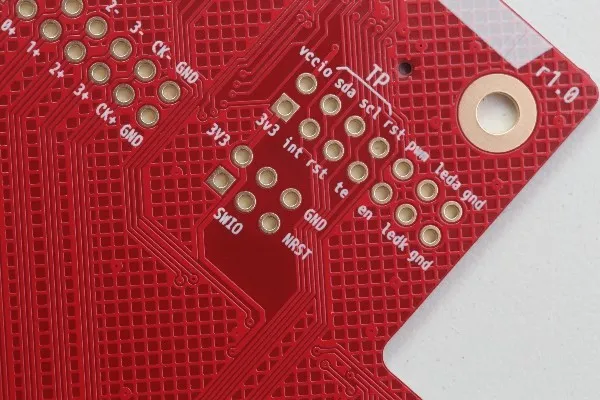
Non-plated through-holes, often abbreviated as NPTH, are essential features in printed circuit board (PCB) design that serve structural and mechanical purposes without requiring electrical conductivity. Unlike their plated counterparts, which facilitate signal routing between layers, non-plated through-holes lack a conductive metal lining, making them ideal for applications such as mounting components, securing PCBs to enclosures, or providing alignment points during assembly. If you have arrived here searching for information on non-plated through-holes, you are likely involved in PCB fabrication, prototyping, or troubleshooting designs where mechanical integrity is as critical as electrical performance. Understanding NPTH can help optimize board layouts, reduce manufacturing costs, and ensure compatibility with automated assembly processes. In practical terms, non-plated through-holes are commonly used for screw holes, fiducials for pick-and-place machines, or ventilation in high-heat environments. Designers should specify NPTH with precise tolerances to avoid issues like drill breakage or misalignment, typically aiming for diameters between 0.5mm and 5mm depending on the application. Best practices include incorporating them early in the design phase using CAD software like Altium or Eagle, and verifying their placement against industry standards such as IPC-7351 for land patterns. This approach not only enhances durability but also minimizes rework during production. For instance, in consumer electronics, NPTH enable robust mounting without interfering with trace routing, while in industrial PCBs, they support heavy-duty fastening to withstand vibrations. By delving into the articles grouped under this tag, you can gain deeper insights into real-world implementations, such as integrating NPTH in multilayer boards or comparing them to vias in high-density designs. These resources offer guidance on common pitfalls, like ensuring sufficient annular ring clearance to prevent solder mask encroachment, and tips for collaborating with manufacturers to achieve optimal results. Whether you are refining a prototype or scaling up production, the knowledge here equips you with the tools to make informed decisions in your PCB projects.
Video Guide

Technical Articles