







-
 00:59
00:59
PCB Rounded Corners: Stop Cracking with Radius
Sharp 90° PCB corners can create stress concentrations that increase the risk of cracking, chipping, and edge damage during depaneling, handling, and assembly. This video explains how adding rounded corners with an appropriate radius can distribute mechanical stress and improve board durability. It covers practical radius recommendations for different board sizes, the impact of radius selection on available board space, and the importance of matching the design to CNC routing capabilities. The video also highlights proper clearance between board edges and copper, traces, or components. These simple mechanical design practices help improve manufacturing reliability across FR4, industrial control, and consumer electronics PCB applications.
-
 00:56
00:56
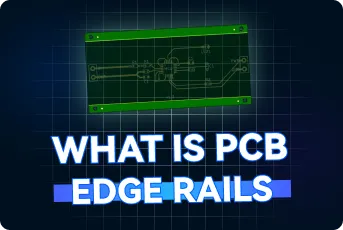
PCB Edge Rails: Why Extra Edges Are Essential for Reliable SMT Handling
PCB edge rails are essential manufacturing features that improve board stability and handling during automated SMT assembly. This video explains why manufacturers add non-functional rails to provide conveyor support, protect components from machine contact, and enable reliable high-speed placement. It covers practical design considerations such as rail width, component clearance, fiducial and tooling-hole placement, and the use of V-cut, mouse bites, or tab routing for final separation. Proper edge-rail design helps reduce handling defects, improve assembly stability, and increase first-pass yield across PCB prototype and volume production.
-
 00:52
00:52
Flexible PCB vs Rigid PCB: Manufacturing Differences That Matter
Flexible PCBs are not simply thinner versions of traditional rigid boards — they require specialized materials and manufacturing processes to achieve reliable bending performance. This video explains the key differences between flexible and rigid PCB fabrication, including the use of polyimide substrates, coverlay protection instead of conventional solder mask, selective stiffener bonding, and precision punch processing for final outlines. It also highlights how these manufacturing techniques enable flexible circuits to withstand repeated movement while maintaining electrical reliability. Understanding these process differences helps engineers choose the right solution between custom flex PCB and rigid-flex PCB designs for demanding applications such as medical devices, automotive electronics, and compact IoT systems.
-
 00:55
00:55
PCB Diode Operation: Understanding PN Junctions and Polarity
Diodes are fundamental semiconductor components that control the direction of current flow and protect electronic circuits from reverse polarity and other electrical faults. This video explains how a diode works by exploring the PN junction, the movement of electrons and holes, and the effects of forward and reverse bias on current conduction. It also highlights the importance of correct diode orientation during PCB assembly, including how the cathode marking ensures proper installation and reliable circuit operation. By understanding these principles, engineers can improve design reviews, DFM decisions, and assembly quality while enhancing the reliability of power supplies, automotive, industrial, and other PCB applications.
-
 00:52
00:52
PCB LED: What Is That Tiny Light on Your Circuit Board?
LEDs (Light Emitting Diodes) are among the most common components on printed circuit boards, serving as power, status, and diagnostic indicators in countless electronic products. This video explains how LEDs work, why they require correct polarity and current-limiting resistors, and the differences between through-hole and surface-mount (SMD) packages. It also explores how semiconductor materials determine LED color and highlights key design and assembly considerations that affect manufacturability, reliability, and long-term performance. By understanding proper LED selection, orientation, and protection, engineers can create more reliable PCB designs and improve assembly quality for consumer electronics, industrial control systems, IoT devices, and other applications.


