










Flexible PCB vs Rigid PCB: Manufacturing Differences That Matter
What This Video Covers
This video explains the core manufacturing differences that separate a flexible PCB from a conventional rigid board. It is not simply a thinner version of FR4 technology. Flexible circuits use polyimide substrates and a specialized coverlay instead of traditional solder mask so the copper traces remain protected while the board repeatedly bends. Selective stiffeners are added only under connectors and components to create rigid zones without sacrificing overall flexibility. The final outline is formed by precision punch press rather than standard routing, followed by electrical testing and visual inspection. These processes enable reliable dynamic flexing in medical devices, automotive electronics, and compact IoT assemblies. Engineers evaluating whether a custom flex PCB or hybrid rigid-flex board better meets mechanical requirements will find clear process insights. For accurate costing, request a flexible PCB quote after reviewing the design considerations shown.
Key Highlights
- Flexible PCBs replace traditional solder mask with coverlay film that protects copper while permitting continuous flexing without cracking.
- Stiffeners are selectively applied only under connectors and components, delivering local rigidity without limiting the bend zones.
- Final board outline is created by precision punch press, then subjected to full electrical testing and visual inspection to guarantee long-term bend reliability.
Coverlay vs Solder Mask – The Flexibility Protection Layer
A conventional rigid PCB relies on solder mask to protect copper traces and define solderable pads. On a flexible circuit this layer would crack under repeated bending. Instead, manufacturers apply a polyimide coverlay film that is laser- or mechanically cut and laminated under controlled heat and pressure. The coverlay bonds directly to the copper and substrate, providing both electrical insulation and mechanical protection while remaining flexible.
Factory practice requires precise coverlay opening registration. Misalignment of even 0.1 mm can leave copper exposed or create stress risers that initiate cracks after a few thousand bend cycles. Coverlay thickness is typically 12.5 µm or 25 µm polyimide with adhesive; the choice depends on required bend radius and environmental sealing needs. In high-reliability applications such as implantable medical devices or automotive camera modules, coverlay adhesion strength and residual stress after lamination are monitored as critical process parameters.
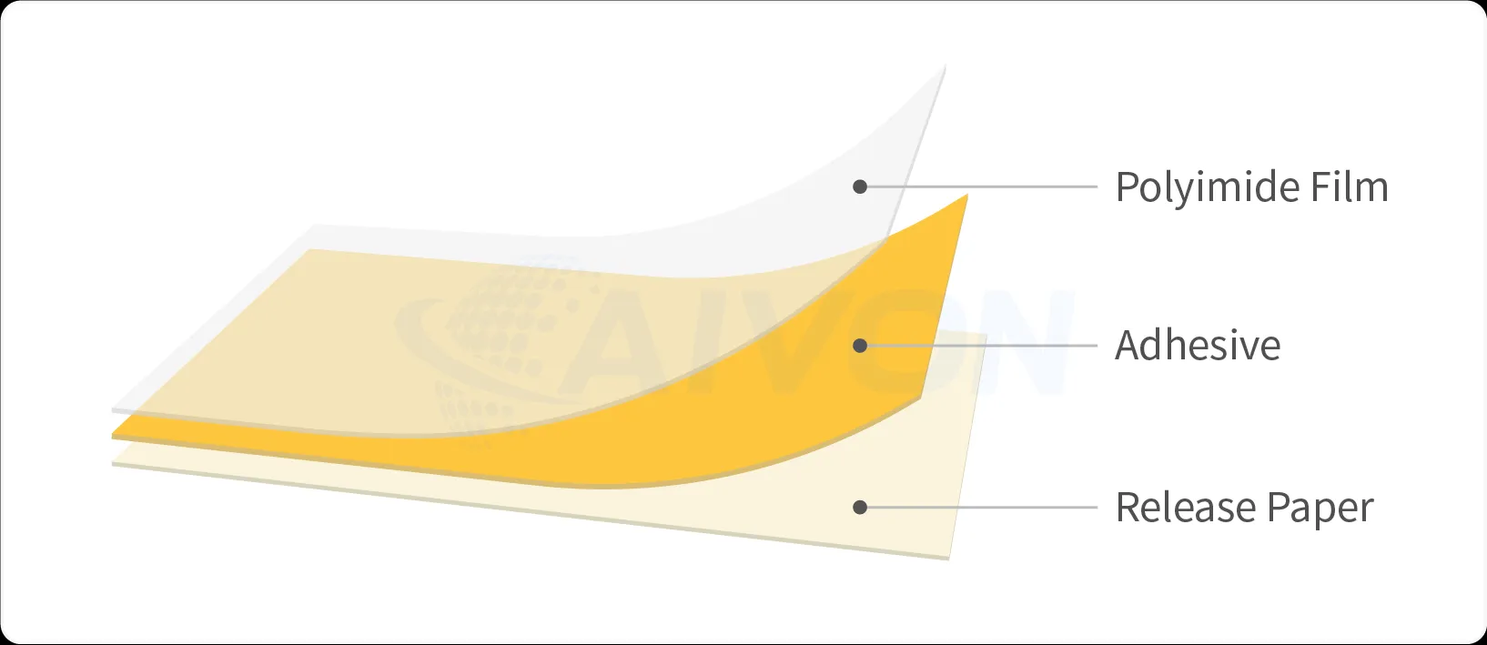
Designers must also specify coverlay openings for components and connectors with adequate clearance for assembly. Insufficient clearance leads to tombstoning or incomplete solder joints during SMT. When the circuit must survive continuous dynamic flexing, the coverlay edge should be kept away from the neutral bend axis to minimize peeling forces.
Strategic Stiffeners – Strength Only Where Components Demand It
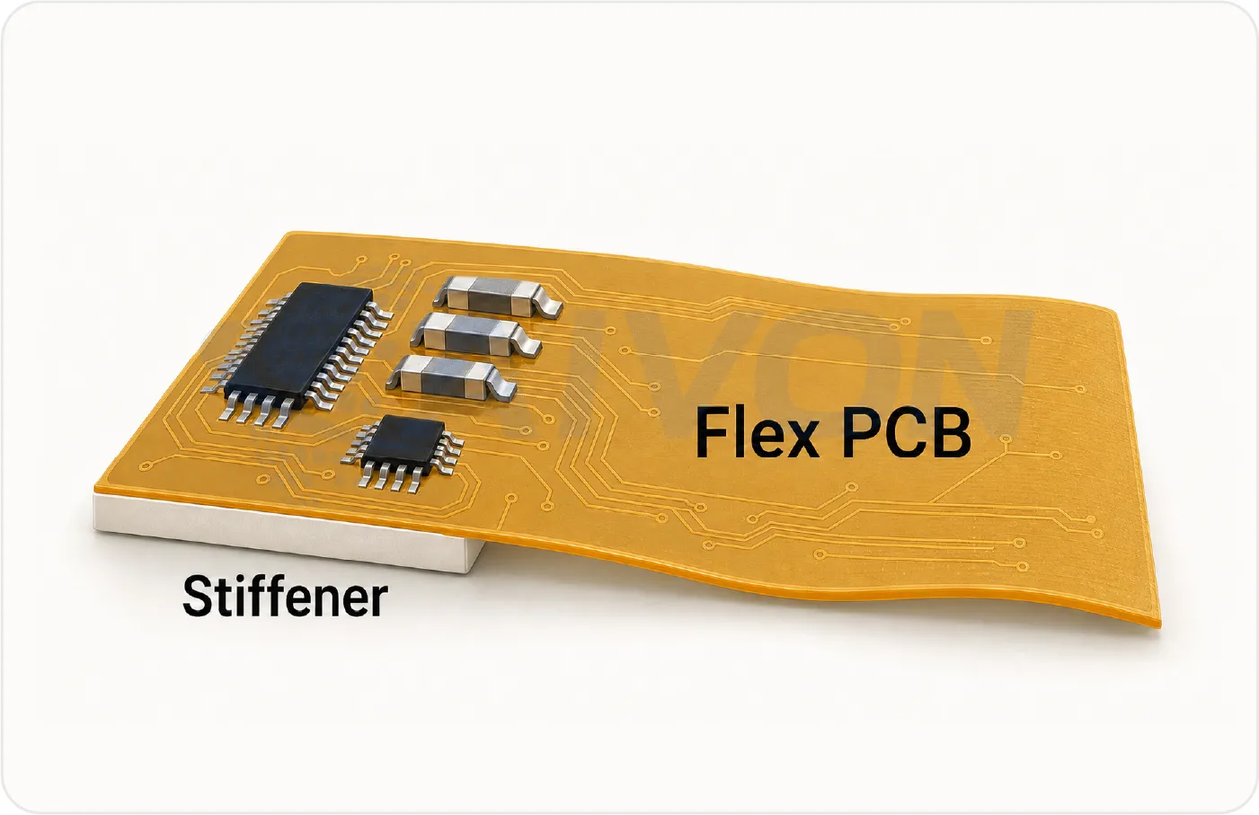
Not every area of a flexible PCB is intended to bend. Connector landing zones, BGA footprints, and areas carrying heavy components require local reinforcement. Stiffeners—usually FR4, polyimide, or stainless steel—are selectively bonded to the opposite side of the flex circuit. Thickness and material are chosen according to the mechanical load and the required flatness for assembly.
A common failure mode occurs when stiffeners are placed too close to the dynamic bend zone. The abrupt transition creates a stress concentration that can fracture copper traces after repeated cycling. Best practice keeps a minimum 0.5–1.0 mm clearance between the stiffener edge and the start of the bend radius, depending on copper weight and layer count. Adhesive selection is equally important: pressure-sensitive adhesives simplify assembly but may creep under elevated temperature, while thermoset adhesives offer higher reliability at the cost of more complex lamination.
In production, stiffener placement accuracy is verified by AOI after bonding. Misplaced stiffeners shift the neutral axis and alter the intended bend behavior, leading to early fatigue. For multi-layer flexible circuits the stiffener stack-up must also consider coefficient of thermal expansion mismatch to avoid warpage during reflow.
Flexible PCB vs Rigid PCB – Manufacturing & Performance Comparison
| Parameter | Rigid PCB (FR4) | Flexible PCB (Polyimide) |
|---|---|---|
| Base Material | Glass-reinforced epoxy | Polyimide film |
| Protective Layer | Solder mask | Coverlay film |
| Outline Formation | CNC routing or V-scoring | Precision punch press |
| Bend Capability | None (static only) | Dynamic or static flex |
| Stiffener Use | Not required | Selective reinforcement under components |
| Typical Thickness | 0.8–1.6 mm | 0.05–0.3 mm (excluding stiffeners) |
| Key Reliability Focus | Thermal cycling, vibration | Bend cycle life, crease resistance |
| Common Applications | Motherboards, power supplies | Wearables, medical sensors, foldable displays |
This comparison highlights why substituting a flexible circuit for a rigid board is never a drop-in change. The entire fabrication sequence—material selection, coverlay lamination, stiffener bonding, and outline punching—must be engineered around the mechanical duty cycle the product will experience.
Design Rules That Prevent Flex Circuit Failure in Real Applications
Successful flexible PCB designs begin with accurate definition of static versus dynamic bend zones. Dynamic regions require rolled annealed copper and controlled bend radius (typically ≥6–10× circuit thickness for single-sided constructions). Trace routing should follow the bend axis rather than cross it perpendicularly; when crossing is unavoidable, hatched copper planes or teardrop pads reduce stress concentration.
Copper weight selection balances current-carrying capacity against flexibility. ½ oz or 1 oz copper is preferred for dynamic flex; heavier copper increases stiffness and reduces cycle life. Coverlay and adhesive thickness must be included in the total stack-up calculation used for bend-radius verification. Finally, the transition from stiffener to free flex area should be gradual—abrupt steps invite cracking.
When these rules are ignored, field failures typically appear as open circuits after a few thousand cycles or as intermittent contact under vibration. Early collaboration with the fabricator during DFM review remains the most effective way to avoid costly redesigns later in the program.
FAQ
Q1: When should I choose a flexible PCB instead of a rigid board for a new product?
A1: Select flexible PCB technology when the design requires repeated bending, three-dimensional packaging, or significant weight and space reduction. Typical decision points include wearable devices, camera modules that fold during assembly, and medical sensors that must conform to body contours. If the circuit remains completely static and has no space constraints, a standard rigid FR4 board is usually more cost-effective.
Q2: How does coverlay thickness affect bend performance and assembly yield?
A2: Thinner coverlay (12.5 µm) improves flexibility and reduces overall circuit thickness but offers less mechanical protection and can be more difficult to handle during SMT. Thicker coverlay (25 µm or more) increases durability at the expense of tighter minimum bend radius. Assembly yield improves when coverlay openings provide adequate clearance for solder paste and component leads—typically 0.1–0.15 mm per side beyond the pad dimension.
Q3: What is the typical cost difference between a flexible PCB and an equivalent rigid board?
A3: Flexible circuits generally cost 2–5× more than comparable rigid boards because of specialized materials (polyimide), coverlay processing, selective stiffeners, and lower panel utilization. The premium narrows on higher volumes and when the flex circuit eliminates connectors or enables a simpler mechanical assembly. Always request a formal flexible PCB quote that includes stiffener and coverlay options for accurate comparison.
Q4: Can stiffeners be added after the flexible circuit is already fabricated?
A4: Stiffeners are normally bonded during the fabrication process under controlled temperature and pressure. Post-fabrication stiffener attachment is possible with pressure-sensitive adhesives but offers lower reliability under thermal cycling and vibration. For production programs, specify stiffener locations and materials at the design stage so they can be integrated into the standard manufacturing flow.
Q5: What bend-cycle life can I realistically expect from a well-designed single-sided flexible PCB?
A5: With proper material selection, trace routing, and bend-radius control, single-sided polyimide circuits commonly achieve 100,000 to several million dynamic bend cycles. Actual life depends on copper type (rolled annealed preferred), total thickness, and whether the bend is continuous or intermittent. Dynamic flex testing to the required cycle count is recommended for any safety-critical or long-life application.
What makes a flexible PCB different from a regular PCB?
It's much more than just a thinner board.
The difference comes from the way it's manufactured.
Unlike rigid PCBs, flexible PCBs go through several specialized processes to handle constant movement.
Flexible PCBs use a Coverlay instead of a traditional solder mask, protecting the copper traces while allowing the board to flex.
But not every part of the board is meant to flex.
Stiffeners reinforce connector and component areas, adding strength only where it's needed.
Next, a precision punch press shapes the board into its final outline before electrical testing and visual inspection.
A flexible PCB isn't designed to bend once—it's engineered to keep working, bend after bend.





