Flexible printed circuit boards require manufacturing processes that can handle thin materials, fine features, complex outlines, and tight alignment requirements. High precision flexible PCB laser manufacturing supports the production of microvias, openings, slots, and flexible circuit outlines while reducing the mechanical stress associated with conventional machining methods.
Laser drilling is commonly used to form small vias in flexible circuits, while flex PCB laser cutting is used for board separation, internal openings, slots, and complex outlines. In addition, flexible PCB lamination affects the final thickness, layer alignment, dimensional stability, and mechanical performance of the FPC.
Highlights
● UV is mandatory for ≤75 µm vias, tight registration, and direct copper ablation; CO₂ suits larger dielectric openings or cost-sensitive coverlay work.
● Aperture tolerance of ±5–10 µm and panel-wide registration accuracy determine plating reliability and yield.
● Residues must be removed by plasma or chemical desmear before electroless copper; incomplete cleaning is a leading cause of open vias and CAF.
● Choose laser type, beam strategy (percussion vs trepanning), and cleaning sequence based on via size, copper thickness, panel stability, and downstream reliability targets.
This article explains the main laser processes used in FPC manufacturing, including laser drilling, laser cutting, lamination considerations, precision control, post-laser cleaning, and common manufacturing defects.
What Is High Precision Flexible PCB Laser Manufacturing?
Why Laser Manufacturing Is Important for Flexible PCBs
Flexible printed circuits are usually built with thin copper foil, polyimide, adhesive layers, coverlay, and other flexible materials. These materials can move, stretch, or deform during manufacturing if they are not properly supported and controlled.
Traditional mechanical tools may create stress, burrs, or dimensional variation when processing fine features on flexible materials. Laser processing uses focused energy without direct mechanical contact, making it suitable for delicate FPC structures and complex designs.
Laser manufacturing can be used to create:
-
Microvias and blind vias
-
Coverlay openings
-
Slots and windows
-
Flexible circuit outlines
-
Fine internal features
-
Local material openings
-
Complex shapes for compact electronic assemblies
The selected laser process depends on the material stack-up, copper thickness, feature size, required accuracy, and production volume.
Which FPC Processes Use Laser Technology?
Laser technology may be used at different stages of flexible PCB production. The most common applications include laser drilling, dielectric opening, outline cutting, slot processing, and local material removal.
Laser drilling is mainly used to create holes or vias. Laser cutting is used to separate the circuit or form a defined opening. In some designs, laser processing may also be used to open coverlay or remove selected dielectric areas before subsequent manufacturing steps.
Each process requires its own parameter settings and inspection criteria. A laser setting that works well for drilling may not be suitable for cutting a complete flexible circuit outline.
Why Laser Drilling Became Essential for FPC Microvias
Thin polyimide and flex PCB adhesive behave differently under a spinning carbide bit than rigid FR-4. The bit flexes, the soft dielectric tears, copper burrs form on the exit side, and heat from friction can locally degrade the polyimide. Minimum practical diameters sit near 150–200 µm; aspect ratios stay modest. Once designs call for blind microvias, via-in-pad, or capture pads under 200 µm, mechanical drilling becomes a yield limiter.
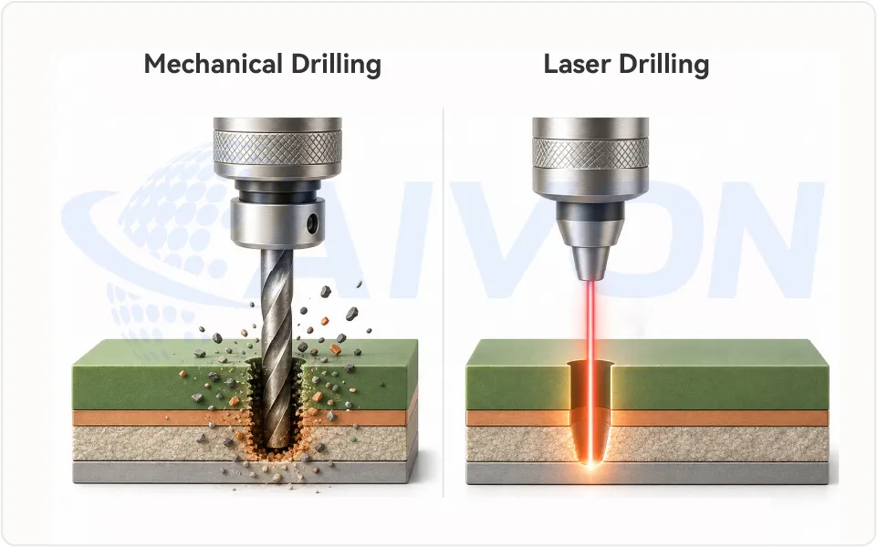
Modern FPCs need exactly those features. Wearables and medical devices push interconnect density; automotive flex circuits demand reliable thermal and signal vias under vibration and temperature cycling; foldable and dynamic-flex applications require clean sidewalls that survive repeated bending. Laser drilling delivers non-contact energy that selectively ablates polyimide and copper without mechanical stress. It forms both through and blind microvias, supports sequential build-up, and produces the tapered or near-straight profiles that plate reliably.
Material realities reinforce the shift. Low glass-transition polyimide, residual adhesive layers, copper thickness variation across a panel, and the inherent dimensional instability of large flex panels all work against mechanical tools. Laser energy can be tuned to the absorption characteristics of each layer, limiting the heat-affected zone and leaving a surface that, after proper cleaning, accepts electroless copper.
Industry practice has adapted rigid-board HDI laser methods to flex as part of the evolving FPC manufacturing process. Typical finished microvia diameters now demanded on production FPCs fall in the 30–80 µm range, with aspect ratios managed carefully. The result is denser routing, smaller packages, and better high-frequency performance through shorter vias and reduced stubs.
Laser Drilling Methods for Flexible PCB
Four approaches dominate production FPC work.
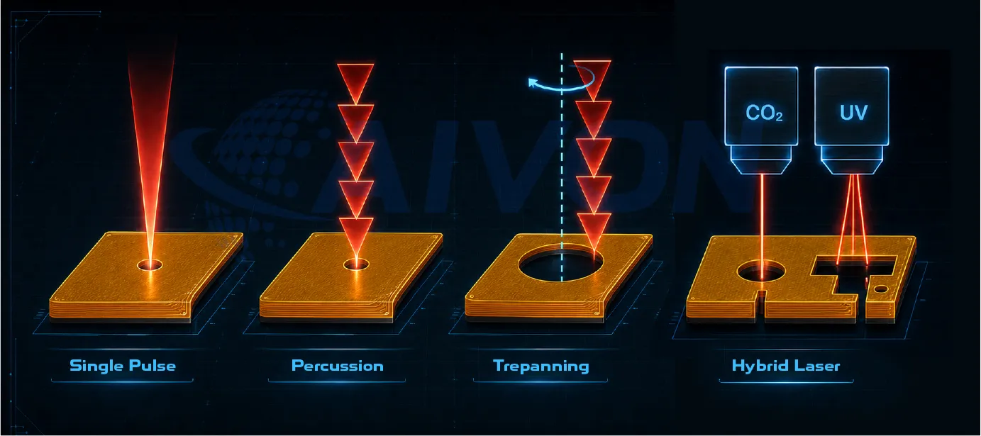
Percussion drilling
Percussion drilling keeps the focused beam stationary while delivering a controlled number of pulses. Each pulse removes a thin layer of material. The method is fast and works well when the finished via diameter is close to the focused spot size. Depth is controlled by pulse count and energy. Percussion is the default for the smallest microvias on thin polyimide stacks because it minimizes cycle time and still produces acceptable roundness.
Trepanning
Trepanning (or spiral/orbit drilling) moves the beam in a circular or spiral path while pulsing. The effective hole diameter becomes independent of the spot size, so larger vias can be opened with a small, high-quality beam. Sidewalls are smoother and more vertical, which improves plating uniformity. Trepanning takes longer per via but is preferred when roundness, taper control, or higher aspect ratios are critical.
Hybrid Laser Drilling
Sequential and hybrid methods combine UV and CO₂ or UV and chemical etching. A common production sequence opens the copper with UV, then clears the dielectric with CO₂ for speed. Dual-step UV—high-energy pulses for copper followed by lower-energy pulses for polyimide—is also used when only one laser source is available. These approaches trade a second process step for better copper-edge quality and reduced risk of overhang.
Choice of method is driven by via diameter, stack thickness, required sidewall quality, and panel volume. Process engineers normally lock the method during coupon development and keep it fixed for a given part number.
Single-Pulse Drilling
Single-pulse drilling delivers one high-energy pulse that removes the entire material thickness in a single shot. It is practical only on very thin dielectric layers where the ablation threshold can be exceeded cleanly. The method is extremely fast and produces minimal thermal accumulation, but control of diameter and residual thickness is limited. Any variation in copper or polyimide thickness quickly results in incomplete openings or oversize holes. Single-pulse is therefore reserved for the thinnest adhesiveless constructions and is rarely the primary method on standard FPC stacks.
UV Laser vs CO₂ Laser for Flexible PCB Microvias
Two laser families dominate FPC work. Selection is driven by material absorption, minimum diameter, heat input, and whether copper must be opened in the same step.
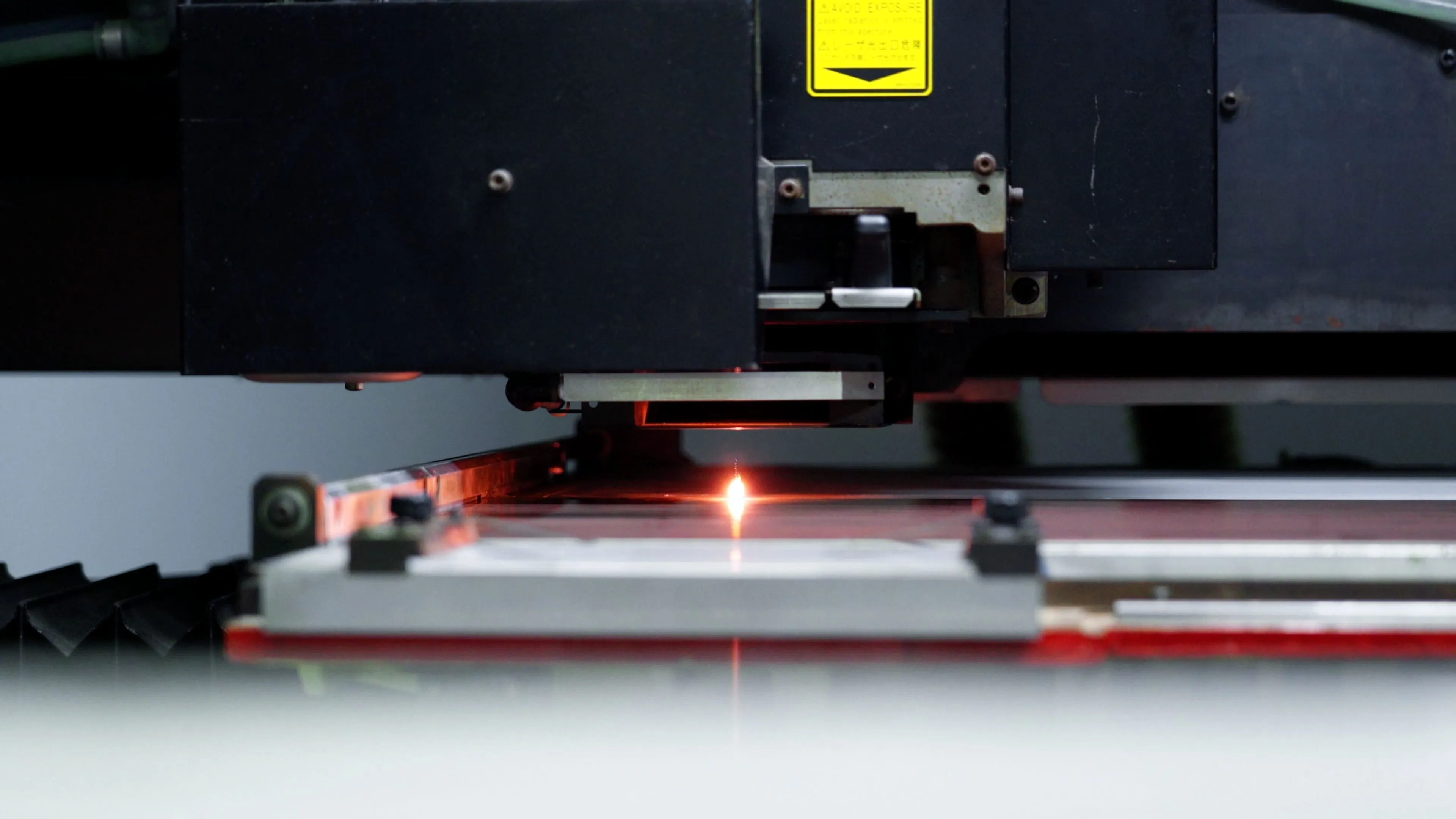
How UV Laser Drilling Works?
UV systems deliver high photon energy. Both copper and polyimide absorb strongly at this wavelength. The absorbed energy drives a combination of photochemical bond breaking and rapid thermal ablation. Material is removed layer by layer with very little lateral heat spread.
The short wavelength allows a tightly focused beam, often 15–40 µm at the work surface. This produces small heat-affected zones, clean copper edges, and well-defined sidewalls. Because copper itself absorbs UV energy, the laser can open copper-clad polyimide in a single process without a prior etch window. Pulse energy, pulse count, and focus position are adjusted so that copper is cleared first, then the dielectric is ablated to the target depth. The result is a microvia whose geometry is controlled primarily by optical and pulse parameters rather than by mechanical tool limits.
How CO₂ Laser Drilling Works?
CO₂ systems rely primarily on thermal ablation. Organic layers absorbthe energy efficiently and vaporize. Copper, however, reflects most of the infrared radiation. Direct CO₂ percussion through copper-clad material therefore leaves overhangs, irregular openings, and inconsistent hole geometry that are difficult to plate.
In practice, CO₂ drilling on copper-clad FPC is performed only after a copper window has been opened chemically (conformal mask) or after a UV step has cleared the metal. Once the dielectric is exposed, CO₂ energy can clear polyimide quickly and with high throughput. The longer wavelength limits the minimum practical focus diameter, so finished vias are typically larger than those produced by UV. Heat-affected zones are also larger, and residual carbonization can be more pronounced if energy is not carefully controlled.
|
Characteristic |
UV Laser |
CO₂ Laser |
|---|---|---|
|
Absorption on Cu/PI |
Strong on both |
Weak on Cu, strong on PI/adhesive |
|
Min practical diameter |
30–50 µm typical, sub-50 µm achievable |
Usually >75 µm |
|
Aspect ratio capability |
Higher for fine vias |
Moderate, dielectric-focused |
|
Heat-affected zone |
Very small |
Larger, more thermal |
|
Residue profile |
Less carbonization if tuned |
More thermal residue possible |
|
Copper drilling |
Direct ablation possible |
Requires conformal mask or sequential UV |
|
Throughput for fine vias |
Moderate; multi-beam helps |
Higher for larger dielectric openings |
|
Typical use |
Fine-pitch HDI microvias, copper-clad FPC |
Coverlay openings, larger through-holes |
When vias must stay at or below 75 µm, registration is tight, or the stack is copper-clad polyimide that cannot tolerate a separate etch-open step, UV Laser FPC processes are the practical choice. CO₂ remains useful and more economical for larger openings, pure dielectric removal after a copper window has been etched, or high-volume FPC coverlay processing. Hybrid sequences (UV open copper, then CO₂ clear dielectric, or dual-step UV) appear in production when throughput and quality both matter.
Equipment cost and maintenance favor CO₂ for simpler dielectric work, while UV platforms carry higher capital and optic costs but deliver the precision modern flex designs require. In practice, many high-mix FPC lines keep both capabilities.
AIVON Laser Drilling Machine Specifications
|
Category |
Specification |
|---|---|
|
Laser Power |
>100 W |
|
X-Y Motion Platform |
AC Servo Linear Motor |
|
Machine Base |
High-Precision Granite Platform |
|
Processing Area |
750 × 850 mm |
|
CCD Alignment Accuracy |
±5.5 μm |
|
X-Y Positioning Accuracy |
±2 μm |
|
X-Y Repeatability |
±2 μm |
|
Overall Machine Accuracy |
<30 μm |
|
Power Supply |
AC 220 V, 50 Hz, <5 kW |
|
Supported File Format |
DXF |
|
Ambient Temperature |
Constant 24°C |
|
Relative Humidity |
≤65% RH (Non-condensing) |
|
Number of Worktables |
Single Platform |
|
Machine Weight |
3,000 kg |
|
Machine Dimensions |
1600 (L) × 2070 (W) × 1850 (H) mm (excluding the signal tower light) |
Key Benefits of AIVON Laser Drilling
● Save Time: Up to 5× faster than conventional drilling for high-hole-count jobs.
● Save Cost: Higher yield and reduced scrap lower overall FPC manufacturing costs.
● Save Labor: Automated precision drilling minimizes manual intervention.
● Peace of Mind: Burr-free, taper-free holes with stable dimensional accuracy improve downstream assembly reliability.
Controlling Aperture and Registration Accuracy in Flex PCB Laser Cutting
Precision is not optional. Aperture typically targets ±5–10 µm. Too large and the capture pad design rules break or plating thickness thins; too small and the via resists plating or creates high resistance. Positional accuracy must stay inside the annular-ring budget across an entire production panel. Roundness, taper angle, and sidewall texture directly affect electroless copper adhesion and long-term reliability.
Several variables dominate control. Laser drilling parameters include pulse energy, pulse width, repetition rate, number of pulses, focus position relative to the surface, and beam quality (M²). Percussion drilling is fast for smaller holes; trepanning (beam orbit) improves roundness and wall quality on larger or higher-aspect features.
Material and stack-up effects are equally important. Copper thickness variation, polyimide thickness tolerance, residual adhesive flow, and built-in stress from prior lamination all shift the ablation threshold and final diameter. Panel stretch or shrinkage between imaging and drilling is common on large flex panels; humidity and temperature history matter.
Common Defects in Flexible PCB Laser Manufacturing
|
Defect |
Cause & Solution |
|---|---|
|
Oversize or undersize holes |
Point to pulse energy or focus drift — tighten process windows and monitor beam power. |
|
Elliptical shape |
Often traces to beam quality, galvo calibration, or panel movement. |
|
Residual copper or incomplete dielectric removal |
Signals insufficient energy or wrong pulse count. |
|
Carbonization or heavy residue |
Indicates excess thermal load — reduce energy or increase assist-gas flow. |
|
Misregistration |
Usually caused by material movement or vision-alignment limits; local fiducials and controlled panel size help. |
While laser drilling defects require precise thermal and optical calibration, maintaining high yield across flexible circuits requires a holistic quality control strategy. For a broader breakdown of fabrication issues beyond microvia drilling, explore our comprehensive guide on
Post-Drill Cleaning and Desmear for Laser-Drilled Microvias
Laser ablation leaves residues: carbonized polyimide fragments, copper oxides, and redeposited material on the sidewalls and pad surface. These residues block electroless copper nucleation and create plating voids or weak adhesion. Long-term reliability suffers through conductive anodic filament (CAF) growth or intermittent opens.
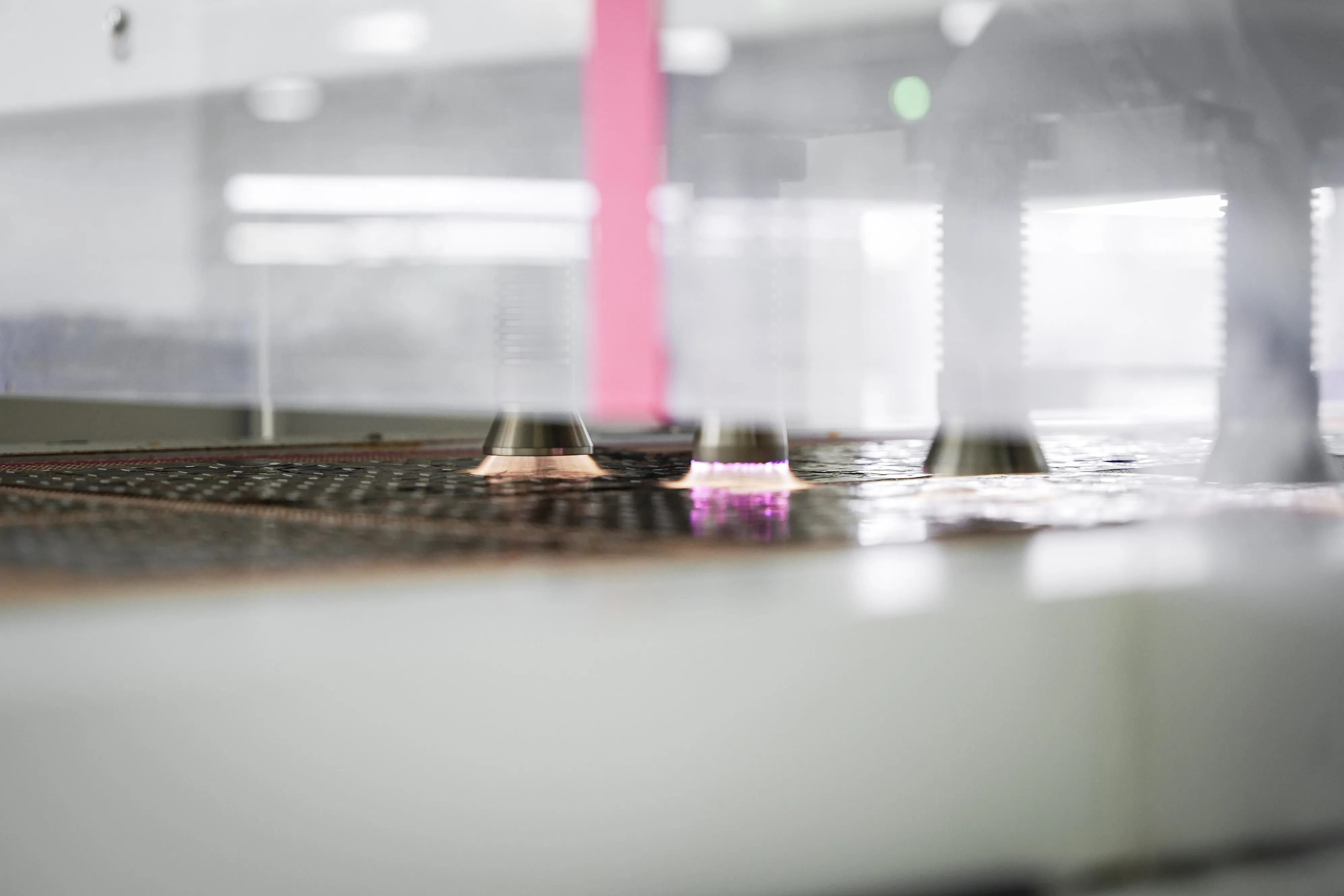
Plasma cleaning is widely used and highly effective on polyimide. Chemical desmear processes adapted from rigid-board practice can also work, though polyimide chemistry differs from epoxy. Ultrasonic aqueous or solvent cleaning removes loose debris; light mechanical conditioning is sometimes applied carefully on the surface.
Material type influences the recipe. Pure adhesiveless polyimide often cleans more cleanly than adhesive-based constructions, where residual adhesive can leave additional smear. Incomplete cleaning is one of the highest-yield-loss modes in high-volume FPC lines. Quality gates after cleaning and after plating catch problems early.
How to Choose the Right Laser Drilling Process for FPC
A practical decision sequence used by process engineers starts with the via itself:
1. Finished diameter and type (blind, through, staggered, or stacked).
2. Stack-up details—copper thickness on each side, dielectric thickness and type (adhesiveless vs adhesive), and any coverlay or stiffener interaction.
3. Registration budget and maximum panel size the design can tolerate.
4. Volume, cost target, and available equipment mix.
5. Downstream plating thickness and reliability requirements (thermal shock, IST, flex cycles, CAF).
UV capital and operating costs are higher, yet the yield improvement on fine-feature work usually justifies them. CO₂ or hybrid routes can reduce cost when diameters allow. Real production challenges appear when moving from prototype coupons to full panels: dimensional stability of large flex sheets, tool-to-tool variation between laser systems, and consistency of the cleaning process across shifts.
At manufacturers with experience across high-density flex, including lines that routinely process polyimide stacks for wearables and automotive modules, the combination of UV capability, disciplined process control, and thorough post-drill cleaning is what turns a capable laser into a reliable production tool.
Laser drilling is not a black-box step. When the process window is understood, the residues are removed, and the registration is controlled, it delivers the microvias that make dense, reliable flexible circuits possible.
Conclusion
High precision flexible PCB laser manufacturing combines laser drilling, laser cutting, material control, lamination stability, and process inspection.
Laser drilling is used to form vias and fine openings, while flex PCB laser cutting supports complex outlines, slots, and windows. Flexible PCB lamination also plays an important role because it affects layer alignment, thickness, panel flatness, and dimensional stability.
For reliable FPC production, laser accuracy should be evaluated together with cleaning, plating, electrical testing, and mechanical requirements. Reviewing these factors early can help reduce process variation and support a smoother transition from prototype production to larger-scale manufacturing.
FAQ
Q1: What size microvias can laser drilling create in FPC?
A1: Production-capable microvia diameters on commercial polyimide copper-clad laminates typically reach 40–50 µm with good process control. Diameters as small as 30 µm are achievable on thinner stack-ups under tightly qualified conditions, although plating reliability and annular ring design become the primary limiting factors rather than the laser itself.
Q2: How does laser drilling affect the dimensional stability of large FPC panels?
A2: The thermal load from laser drilling is highly localized and short in duration, so direct panel shrinkage is minimal. Greater dimensional variation usually results from pre-existing moisture or residual stress in the polyimide, which can cause panel movement between imaging and drilling. Controlled baking, vacuum hold-down, local fiducials, and limiting panel width help maintain registration accuracy.
Q3: Can CO₂ lasers drill copper-clad FPC directly, or is a sequential process required?
A3: CO₂ laser energy is largely reflected by copper, making direct drilling through copper prone to overhang, inconsistent hole geometry, and plating defects. For this reason, manufacturers typically use a chemically etched copper window or a dual-step process combining UV laser drilling followed by CO₂ laser processing.
Q4: What cleanliness level is required before electroless copper plating of laser-drilled microvias?
A4: The microvia sidewalls and via bottom must be free of carbonized residue and oxides before electroless copper plating. Plasma cleaning, typically using O₂ or O₂/CF₄, followed by AOI verification, is commonly required. Any remaining smear or discoloration can cause nucleation defects and plating voids.
Q5: When is trepanning preferred over percussion drilling for FPC vias?
A5: Trepanning is preferred when the finished via diameter is larger than the laser spot size, when superior sidewall roundness and smoothness are required for reliable plating, or when higher aspect ratios demand more controlled energy delivery. Percussion drilling is faster and more suitable for the smallest vias where the laser spot already matches the target diameter.
Q6: Can laser processing be used on both single-layer and multilayer FPCs?
A6: Yes. Laser processing can be used for both single-layer and multilayer flexible circuits. However, the suitable method depends on the layer construction, dielectric thickness, copper arrangement, coverlay, adhesive, and required feature geometry. Multilayer FPCs may require additional alignment and process validation because more layers must remain accurately registered during manufacturing.
Q7: Is laser processing suitable for prototype and mass production FPCs?
A7: Laser processing can support both prototypes and mass production. It is useful for prototypes because it can produce complex openings and outlines without requiring a dedicated mechanical cutting tool. For larger production volumes, the process must be evaluated for cycle time, equipment capacity, material handling, inspection requirements, and repeatability.
Q8: Can laser processing replace mechanical cutting for every flexible PCB?
A8: No. Laser processing is not automatically suitable for every FPC design. Material thickness, copper distribution, board size, edge requirements, production volume, and cost targets all affect process selection. Mechanical cutting, die cutting, or other methods may still be appropriate for certain structures or high-volume applications.
Q9: Does laser processing change the flexibility of an FPC?
A9: Laser processing may affect flexibility if excessive heat damages the polyimide, adhesive, copper, or nearby bend area. The impact depends on the laser parameters, material stack-up, feature location, and distance from dynamic bending zones. Critical bend areas should be reviewed during design and process validation to avoid creating stress concentrations or damaged edges.
Q10: How close can a laser feature be placed to a copper trace?
A10: The allowable distance depends on the laser spot size, process tolerance, material stack-up, copper thickness, heat input, and required electrical clearance. A laser opening or cut that is too close to a trace may expose, weaken, or damage the copper. The final clearance should therefore be confirmed through design review and representative process testing rather than using one universal value.
Q11: Can laser cutting produce internal openings and narrow slots in FPCs?
A11: Yes. Laser cutting can produce internal openings, narrow slots, connector windows, sensor openings, and irregular circuit outlines. The design should account for the minimum feature size, corner geometry, edge quality, heat-affected area, and the distance between the cut path and nearby conductive features.
Q12: What is the difference between laser processing and laser ablation in FPC manufacturing?
A12: Laser ablation removes selected material through controlled energy input, often by vaporizing or breaking down a thin dielectric, adhesive, or coverlay layer. Laser drilling and laser cutting are specific applications of laser processing. The term "ablation" describes the material-removal mechanism, while drilling and cutting describe the intended feature or geometry.
Q13: How should laser-processed FPCs be inspected before shipment?
A13: Inspection should be based on the function and risk of the FPC. Typical checks may include dimensional inspection, laser opening size, cut-line continuity, edge condition, registration, residue, copper exposure, and visual defects. Where required, manufacturers may also perform cross-section analysis, plating evaluation, electrical testing, or mechanical reliability testing.
Q14: What should I do if laser-processed FPCs show burn marks or dark edges?
A14: Burn marks or dark edges may indicate excessive heat input, unsuitable focus, incorrect scanning speed, excessive pulse energy, or insufficient cleaning. The manufacturer should review the material stack-up and laser parameters, inspect the affected area, and confirm whether the discoloration is cosmetic or associated with material damage. Process adjustments should be validated on sample parts before production resumes.
Q15: Does FPC laser manufacturing require a special design review?
A15: A design review is recommended when the FPC includes fine vias, narrow slots, complex outlines, tight registration, thin dielectric layers, or closely spaced copper features. The review should cover the stack-up, laser feature geometry, bend areas, copper clearance, coverlay, stiffeners, tolerances, and downstream plating or assembly requirements. This helps identify manufacturability risks before tooling or production.
Q16: How can I improve the yield of a laser-processed flexible PCB?
A16: Yield can be improved by keeping the material stack-up consistent, controlling lamination variation, defining realistic feature tolerances, maintaining accurate alignment references, stabilizing laser parameters, and using appropriate cleaning and inspection methods. Representative samples should be evaluated before full production, especially when the design combines thin materials with fine laser features.