Most electronic systems are powered by DC supplies. If the supply is accidentally connected in reverse, sensitive components and the entire board can be damaged in an instant. Reverse-polarity protection is therefore a fundamental requirement for robust power-input design.
The simplest technique is a series diode. Its unidirectional conduction prevents reverse current when the supply is connected backward. However, a diode introduces a forward voltage drop. For a silicon diode, this is typically around 0.7 V. At light load this drop may be tolerable, but at higher currents it causes significant power loss and heat. For example, at 1 A a 0.7 V drop dissipates 0.7 W. The resulting temperature rise threatens long-term reliability for the diode itself and for nearby components.
A more efficient approach is to use a MOSFET as an "ideal diode." When fully enhanced, a MOSFET's conduction loss is I2 × Rds(on), not a fixed diode drop. With a low Rds(on) device, the forward voltage can be just tens of millivolts at ampere-level currents, greatly improving efficiency and thermal performance while maintaining robust reverse blocking.
How a MOSFET Implements Reverse-Polarity Protection
A MOSFET contains an intrinsic body diode between its source and drain. Properly orienting this diode and controlling the MOSFET gate with a MOSFET gate driver produces one-way conduction that mimics a diode in forward operation and blocks current when the input is reversed:
- Forward (correct) polarity: The body diode briefly conducts, allowing the output (or return) node to rise. As the voltage at the MOSFET's source changes, the gate-to-source voltage (Vgs) increases through a resistor network and enhances the MOSFET. Once fully on, current flows through the MOSFET channel with very low loss set by Rds(on).
- Reverse polarity: The body diode is reverse-biased, so no current flows. The gate bias collapses such that Vgs remains near 0 V (or of the wrong polarity), keeping the MOSFET off and the load protected.
Two practical single-transistor topologies are commonly used:
- Low-side protection with an NMOS in the return path.
- High-side protection with a PMOS in the positive rail.
The choice between them depends on how the system reference is defined and whether the load must remain referenced to the common ground in forward operation.
NMOS Reverse-Polarity Protection (Low-Side)
In a low-side configuration, an NMOS is placed in series with the return path between the load and ground. The MOSFET's body diode is oriented to conduct from the load return to ground (forward direction), and the gate is biased so the NMOS enhances when the supply polarity is correct. A resistor network (often denoted as R1 and R2) develops the required Vgs from the supply and the MOSFET's source.
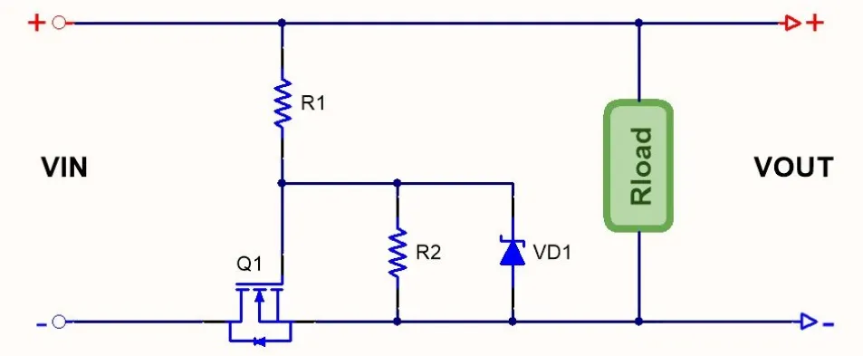
Figure 1 | NMOS reverse-polarity protection circuit. The resistor network biases the gate to enhance the NMOS under correct polarity while the body diode blocks reverse current.
Forward Conduction (Correct Polarity)
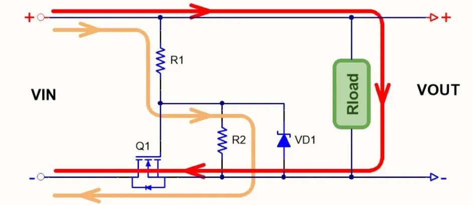
When the supply is connected with the correct polarity (positive at the top rail and negative at the return), the body diode conducts initially. A small current flows through the resistor network and the body diode to ground, pulling the source node close to ground. As a result, the gate-to-source voltage rises above the MOSFET's threshold and the device turns on. Once enhanced, the channel carries the load current with a forward drop approximately equal to I × Rds(on), much lower than the drop across a series diode.
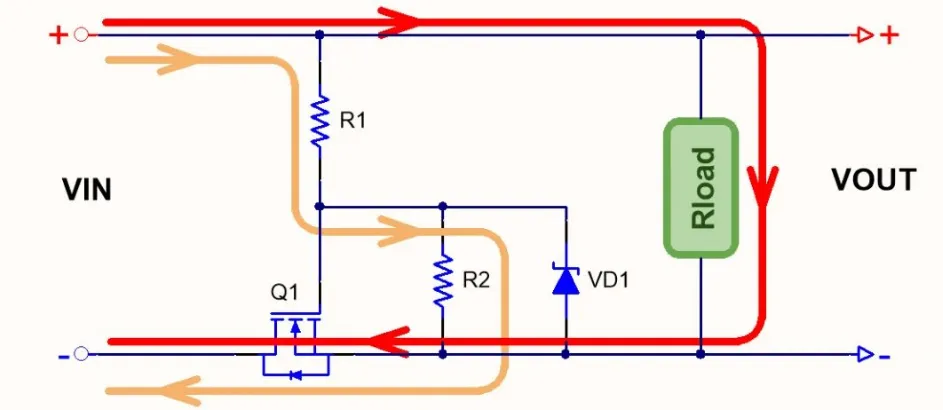
Figure 2 | Forward conduction path. The initial current through the body diode brings the source low enough for Vgs to enhance the NMOS, after which the channel conducts with low loss.
Reverse Polarity Blocking
If the supply is reversed (positive at the return and negative at the top rail), the body diode is reverse-biased. The gate network no longer develops a positive Vgs; the NMOS remains off and the series path is open. The load sees no current, and downstream circuitry is protected from reverse voltage stress.
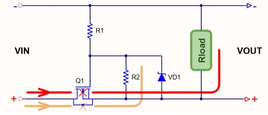
Figure 3 | Reverse-polarity condition. The body diode is reverse-biased, Vgs is not forward-enhancing, and the NMOS remains off, isolating the load.
PMOS Reverse-Polarity Protection (High-Side)
In many systems the ground node is shared across multiple subsystems or interfaces. In those cases, preserving a direct ground reference is important, and placing a switch in the return path is not acceptable. A PMOS on the high side is the simplest solution for reverse protection while keeping ground intact.
With a PMOS on the positive rail, the source connects to the supply input and the drain connects to the load. The PMOS body diode is oriented to conduct from input to load in the forward direction. A gate-bias network ensures that, under correct polarity, the gate is driven below the source enough to enhance the channel. When the polarity is reversed, the body diode is reverse-biased and the gate-source voltage collapses, turning the device off.
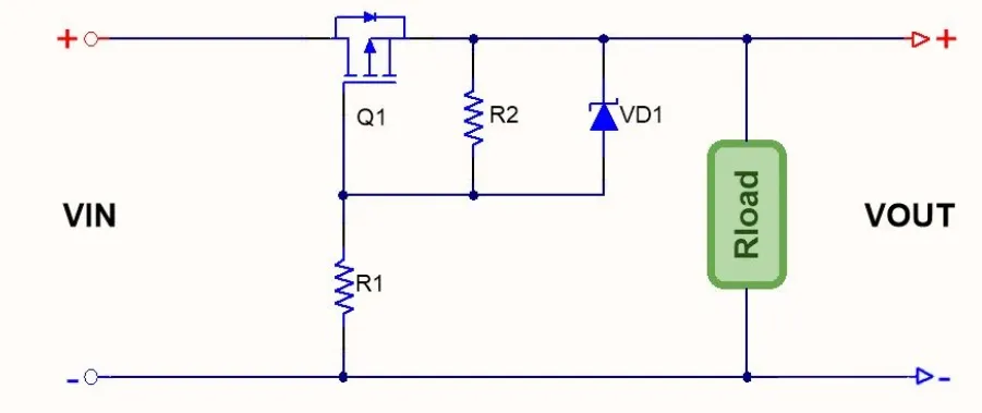
Figure 4 | PMOS reverse-polarity protection circuit. This high-side topology is typically preferred in systems with a common ground.
Selecting NMOS vs. PMOS
- Use a PMOS high-side topology when the system shares a common ground and you must avoid interrupting the ground reference. This is the most common arrangement for DC-powered equipment.
- Use an NMOS low-side topology when the system has a common positive rail or when it is acceptable to switch the return path. This can offer very low Rds(on) with widely available NMOS devices.
While an NMOS can also be used on the high side, doing so requires a gate drive above the input rail (for example, with a charge pump or an ideal-diode controller) to achieve a sufficient Vgs. The simple single-transistor PMOS topology generally remains the most straightforward choice for high-side protection without additional gate-drive circuitry.
Component Selection and Design Considerations
MOSFET Parameters
- Vds rating: Choose a MOSFET with a drain-to-source voltage rating comfortably above the maximum expected input voltage, including tolerances and transients.
- Rds(on): Lower Rds(on) reduces forward conduction loss and heat. Ensure the device's thermal performance (package, junction-to-ambient resistance) supports your worst-case current.
- Vgs(th) vs. enhancement: The gate threshold voltage indicates the onset of conduction at a small current, not full enhancement. Select a device that fully enhances at the gate-source voltage available in your topology (logic-level PMOS/NMOS as appropriate).
- Gate ratings: Respect the absolute maximum ±Vgs rating. In high-voltage inputs, a resistor divider or a clamp (for example, a gate-to-source TVS or zener) may be necessary to keep Vgs within limits.
Gate-Bias Network (R1, R2)
- Purpose: The divider biases the gate relative to the source so that, with correct polarity, Vgs exceeds the required enhancement level, and with reverse polarity, Vgs returns to near 0 V to keep the MOSFET off.
- Values: Use values that balance leakage and noise immunity. Excessively large resistances increase susceptibility to leakage and noise; excessively small resistances waste input current. Keep the gate network power dissipation negligible compared to the load.
- Turn-on speed: A small series resistor in the gate path can control the MOSFET's dV/dt, reducing inrush-induced EMI and gate ringing. This is often sufficient for softening the transition when large output capacitors are present.
Body Diode and Inrush
In forward operation, the body diode conducts briefly until the MOSFET channel turns on. If the load includes large bulk capacitance, this can cause an inrush current spike through the diode and then the channel. Options to mitigate stress include adding an NTC inrush limiter, controlling the MOSFET gate slew rate, or pre-charging downstream capacitance. Ensure the MOSFET's diode and channel can tolerate the transient current profile.
Thermal and Mechanical
- Package and copper: Provide adequate copper area and thermal vias to spread heat. Place the MOSFET near the input connector to limit the length and resistance of high-current paths.
- Current path: Keep the series path (connector → MOSFET → load) short and wide to minimize IR drop. Use multiple vias for transitions between layers.
- Kelvin connections: Where practical, reference the gate network to the MOSFET source with a short connection to avoid spurious Vgs from ground bounce.
Reverse Leakage and Two-FET Configurations
Single-MOSFET reverse-protection circuits exhibit extremely low reverse leakage because the body diode blocks. In applications that require bidirectional blocking or extremely low leakage in both directions under all conditions, a back-to-back MOSFET arrangement (two MOSFETs in series with sources tied together) can be used. This eliminates body-diode conduction in either direction when off, at the cost of extra components and gate-drive complexity.
Practical Design Checklist
- Confirm the required topology: PMOS high-side for common-ground systems; NMOS low-side when switching the return is acceptable.
- Orient the MOSFET so the body diode conducts in the forward (normal) direction and is reverse-biased under reversed input.
- Design the gate-bias network to guarantee sufficient Vgs for full enhancement under minimum input voltage and to never exceed the ±Vgs rating at maximum input.
- Verify worst-case conduction loss: P = I2 × Rds(on). Ensure the device's thermal capability and PCB copper keep junction temperature within limits.
- Evaluate inrush behavior into downstream capacitance. Add gate slew control or inrush limiting if necessary.
- Validate reverse-polarity performance with bench tests: apply reverse voltage within the expected range and confirm negligible reverse current and correct device off-state.
Summary
Replacing a series diode with a MOSFET-based reverse-polarity protection circuit dramatically reduces loss and heat while maintaining robust protection. An NMOS on the low side is effective when switching the return is acceptable, while a PMOS on the high side preserves a common ground and is the most straightforward solution in typical DC systems. With proper MOSFET selection, gate-bias design, and PCB layout, this simple ideal-diode approach delivers efficient, reliable protection against accidental reverse connection.