Flexible PCB manufacturing is a precision fabrication process that transforms polyimide-based materials into reliable flexible circuits through drilling, plating, circuit imaging, etching, coverlay lamination, surface finishing, and final assembly. Unlike rigid PCB fabrication, every stage must account for material movement, multiple thermal cycles, and the mechanical reliability required for repeated bending.
Understanding the complete FPC manufacturing process helps engineers make better DFM decisions, buyers evaluate suppliers more effectively, and project teams identify potential manufacturing risks before production begins. This guide walks through a typical 21-step flexible PCB manufacturing process, explains the purpose of each stage, highlights the most important production control points, and shows how the process differs from conventional rigid PCB manufacturing.
Highlights
● Most single/double-sided FPC lines run a clear 15-20 steps sequence dominated by coverlay lamination, multiple thermal cycles, and stiffener attachment rather than complex multilayer lay-up.
● Critical control points are hole copper thickness, post-compensation line width/space, coverlay and stiffener cure, and ENIG thickness.
● Knowing the real order of plasma, chemical cleaning, cold press, and final dust-film application prevents the most common registration and surface defects.
In this guide you will see a production-realistic 21-step flow, the key process windows that drive yield, differences from rigid PCB manufacturing, and answers to the questions engineers and purchasers ask most often.
What Is the Modern FPC Manufacturing Process?
A flexible printed circuit starts with polyimide film, copper foil, and either adhesive or adhesiveless copper-clad laminate. Finished thickness before stiffeners is often held around 0.1 mm. Coverlay, photosensitive ink, local stiffeners, and a surface finish complete the product. What makes the flexible PCB manufacturing process fundamentally different from rigid FR-4 production is the combination of specialized steps and tighter process windows required by the thin, flexible substrate.
These operations replace the high-pressure, high-temperature lamination and mechanical routing used for rigid boards. The entire sequence prioritizes dimensional stability, adhesion on polyimide, and retention of flex life. As a result, panel sizes are usually smaller, thermal budgets are lower, tension control is constant, and process discipline must be tighter, explaining both the higher unit cost and the longer lead times most buyers observe.
Complete FPC Manufacturing Process Flow
The following sequence reflects the typical production flow used on most single-sided and double-sided FPC lines. Multilayer constructions add inner-layer imaging, oxide treatment, and vacuum lamination steps, but the core logic remains the same. Exact step count varies by factory and product; the order below covers the essential stages from material preparation to final packaging.
Step 1: FPC Material Preparation
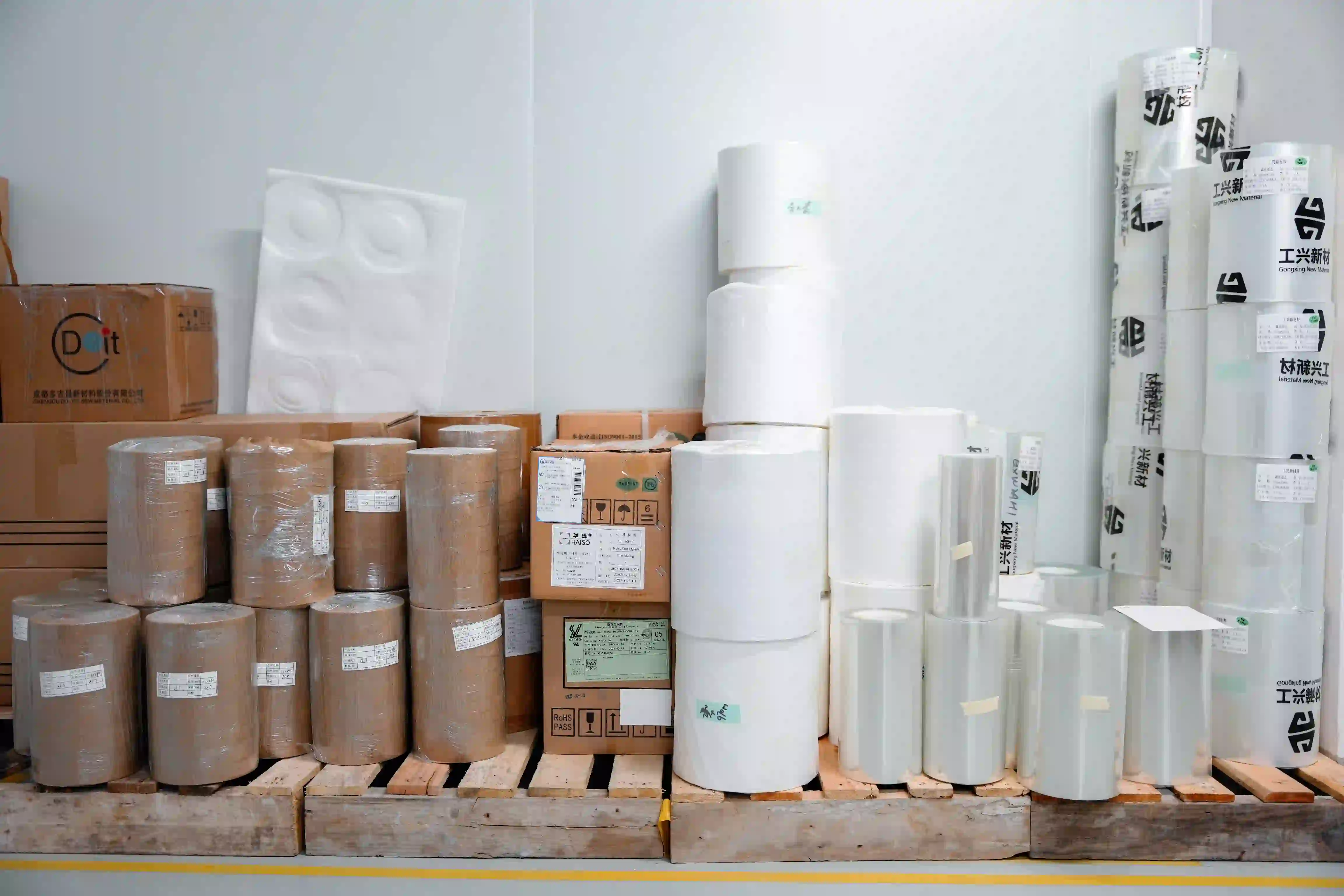
Confirm material specifications, quantity, and batch numbers. Prepare the copper foil and polyimide (PI) base film or copper-clad laminate.
In most factories the starting polyimide thickness ranges from 12 µm to 50 µm for thin flexible circuits, while finished board thickness before stiffeners is commonly held around 0.1 mm. Incoming inspection checks for thickness uniformity, copper adhesion, and dimensional stability so that later process windows remain under control.
In AIVON, the available FPC material thicknesses is as follows:
|
PI Thicknesses |
12.5μm, 25μm, 50μm, and 75μm |
|
Copper Thicknesse |
12μm, 18μm, 35μm, and 70μm |
|
Adhesive Thickness |
Generally 15μm |
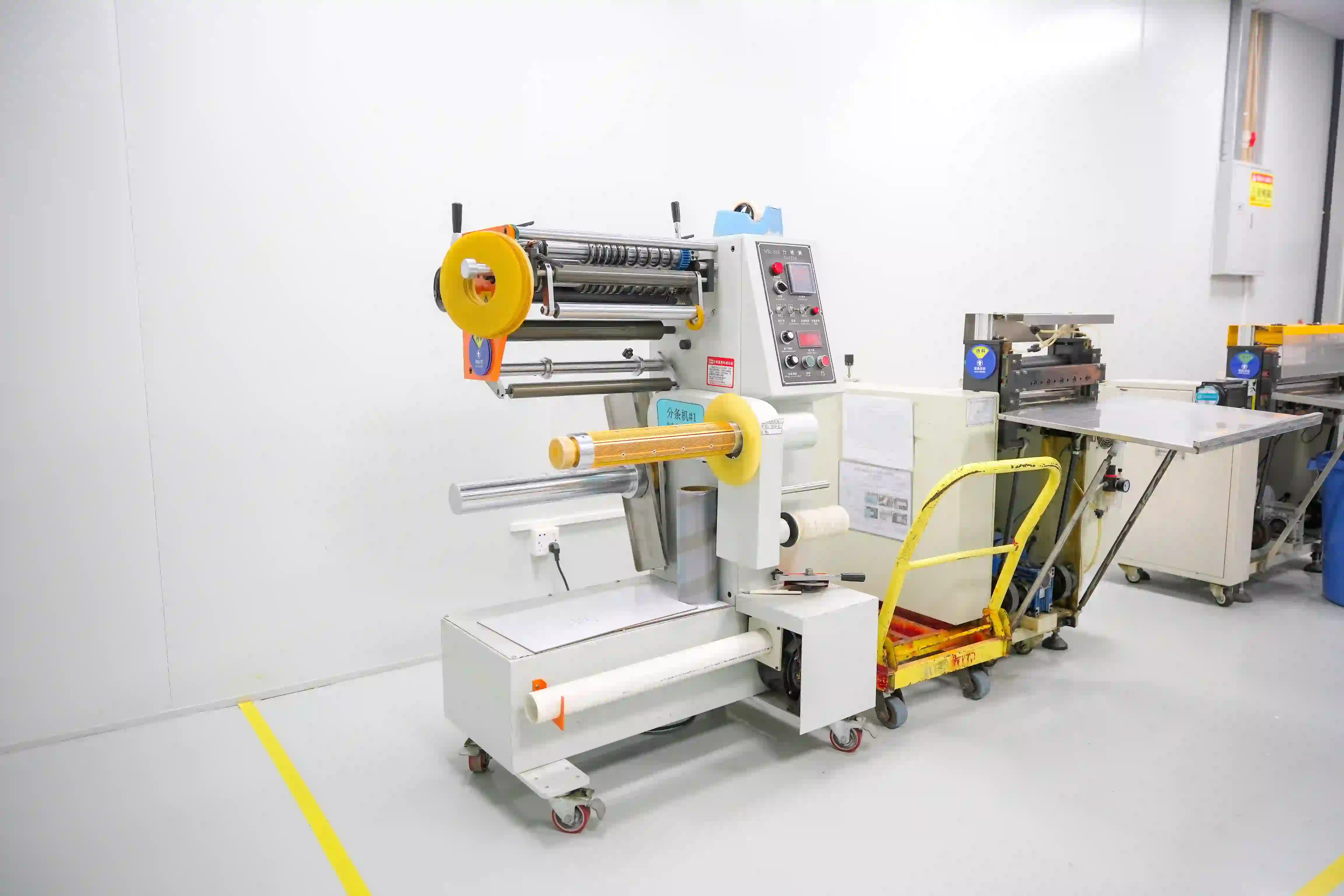
Step 2: FPC Panel Cutting
Cut the copper-clad laminate or polyimide film into production panels according to the job size and panelization plan. Accurate cutting ensures consistent panel dimensions, proper edge quality, and enough process border for subsequent drilling, imaging, and handling. Thin polyimide is easily damaged, so cutting tools and vacuum handling systems must avoid scratches, wrinkles, or edge tears that would become yield losses later.
Step 3: FPC Drilling
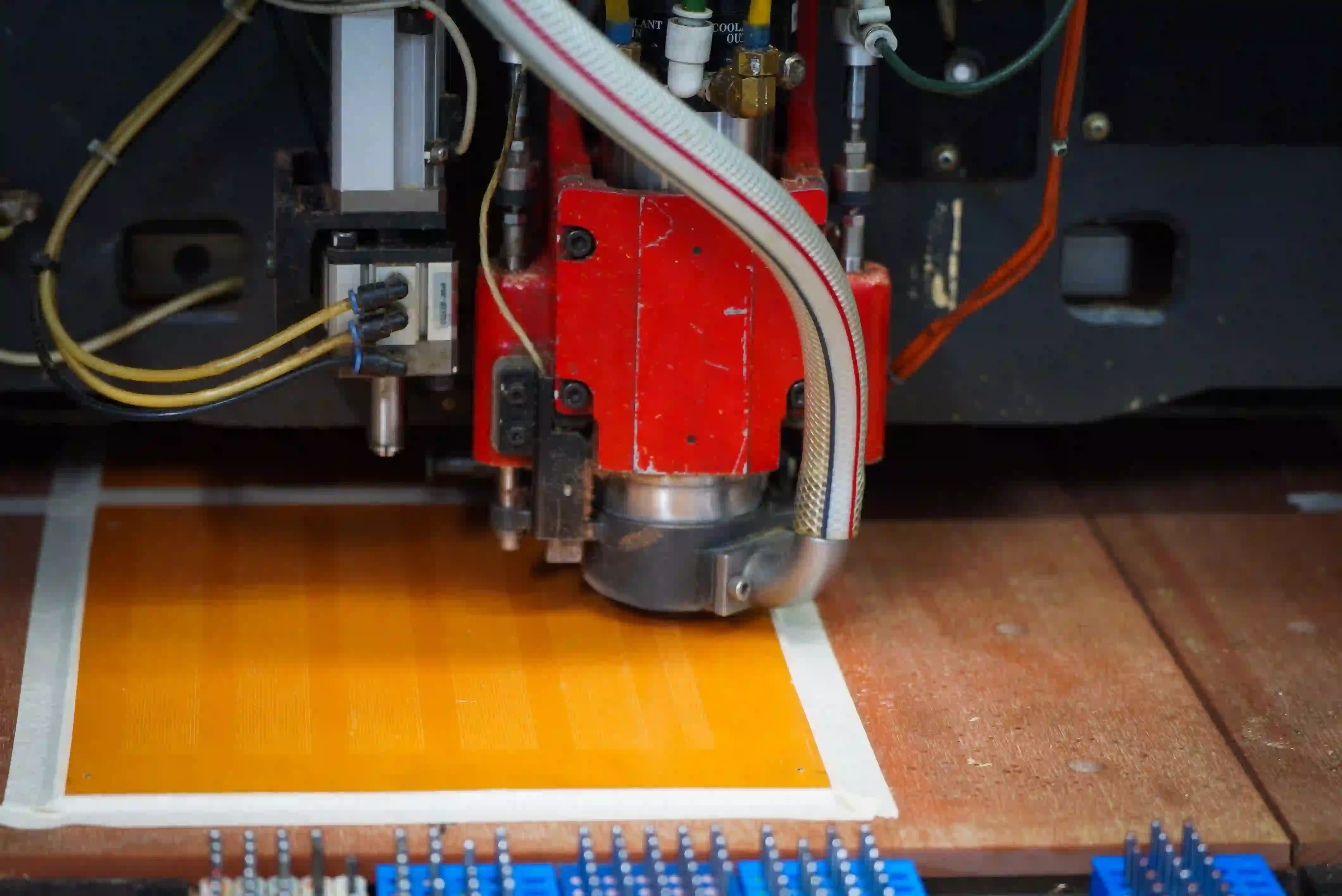
Form through-holes using mechanical or laser drilling according to the drill program. Mechanical drilling is still common for larger holes; FPC laser drilling is preferred when smaller diameters or tighter registration are required. Proper drill parameters and debris removal protect the thin substrate from mechanical stress and residual material that would interfere with plating.
AIVON Capabilities in Drilling:
|
Minimum PTH Hole Aperture |
0.1mm |
|
Hole Aperture Tolerance |
±0.075mm |
|
Finest Pitch Between Adjacent PTH Holes |
0.3mm |
Step 4: Black-Hole and VCP Electroplating
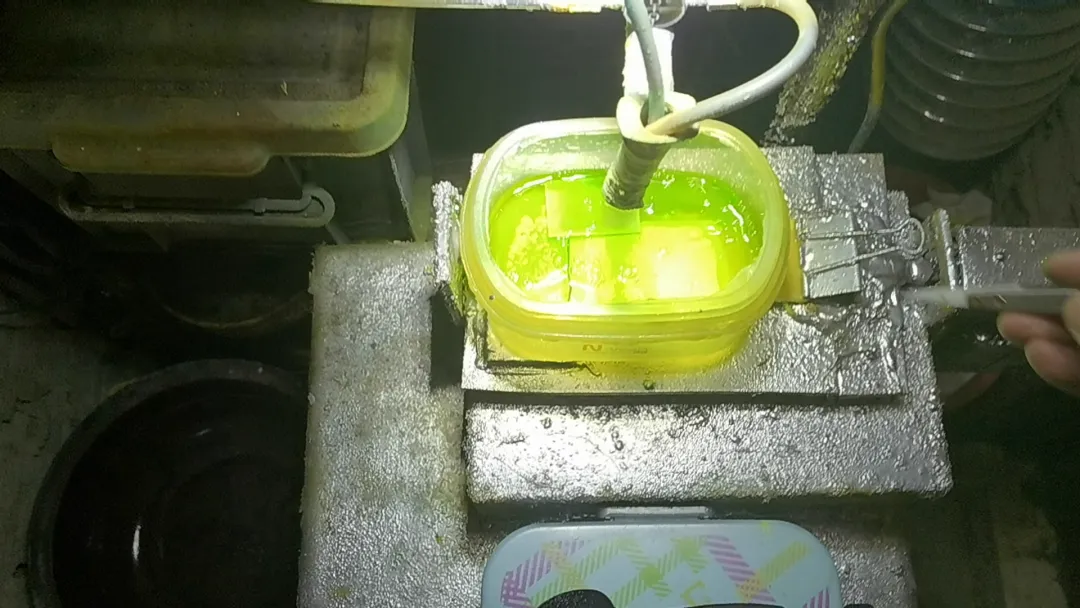
Apply a conductive seed layer, commonly black-hole or electroless copper, followed by electrolytic plating to build copper on the hole walls.
The goal is reliable electrical continuity while keeping the plated copper thin enough to preserve overall flexibility. Surface preparation and plating bath control are critical because polyimide surfaces are more difficult to metallize than epoxy-glass materials.
Step 5: FPC Circuit Imaging (LDI Exposure)
Coat the panel with photoresist and define the circuit pattern by laser direct imaging (LDI). Development removes the unwanted resist, leaving the etch-resistant pattern. Alignment must compensate for the dimensional movement typical of thin polyimide under changes in temperature and humidity.
Step 6: Copper Etching and Resist Stripping
Chemically etch away the unprotected copper and strip the remaining photoresist. Etch chemistry and undercut control are tighter than on rigid boards because fine lines on thin film cannot tolerate large etch bias. Clean stripping prevents residual resist from causing FPC manufacturing defects in later coverlay or ink adhesion.
Step 7: FPC Coverlay Application
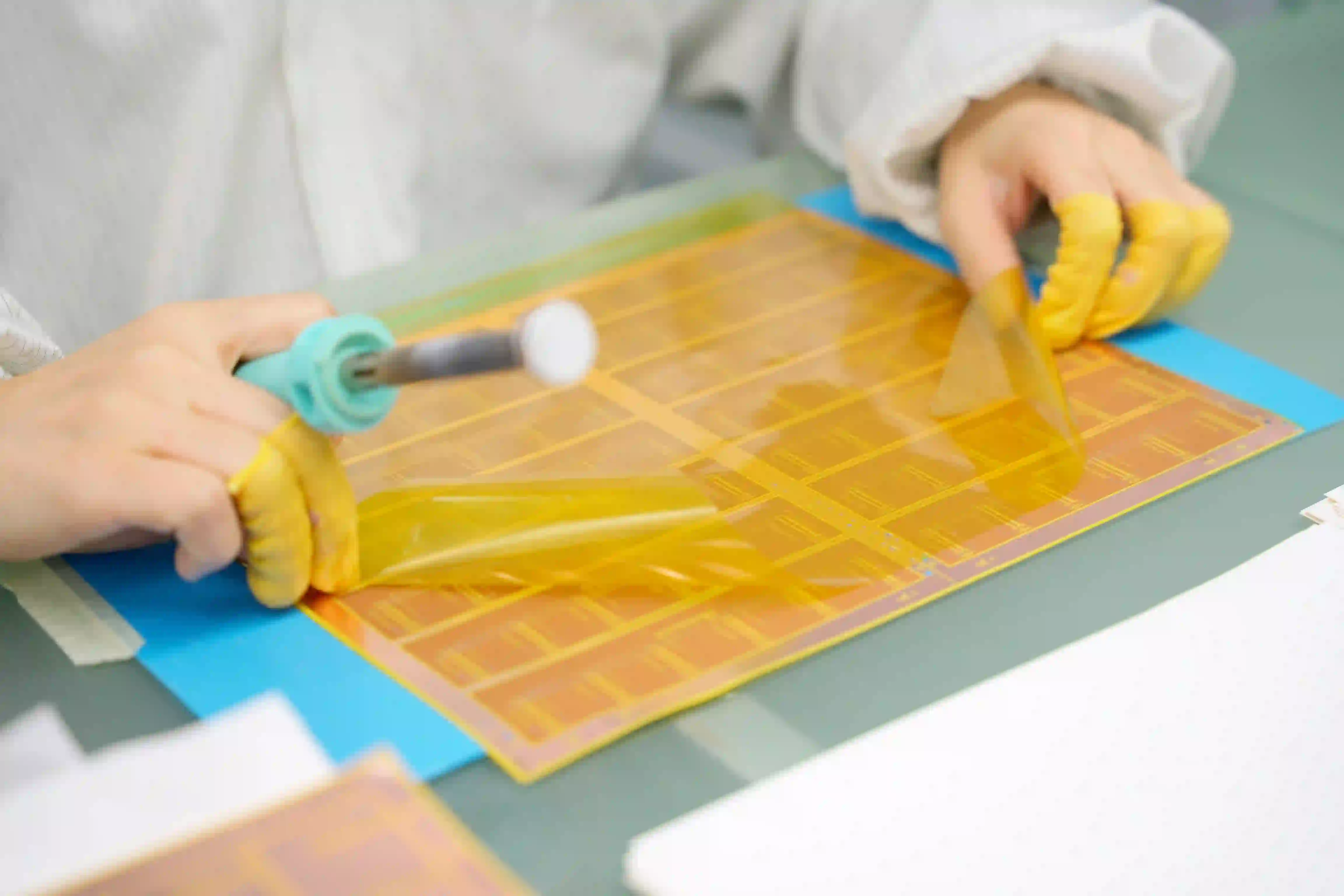
FPC coverlay provides insulation and protects the conductive circuit from mechanical damage, contamination, and environmental exposure. It is typically formed from a flexible dielectric film with adhesive or other bonding structures.
During application, registration between the coverlay openings and the underlying pads is critical. Poor alignment can reduce pad exposure or affect solderability. For designs with repeated bending, coverlay selection and bonding conditions also influence flex reliability.
Step 8: Cold Press and Coverlay Curing
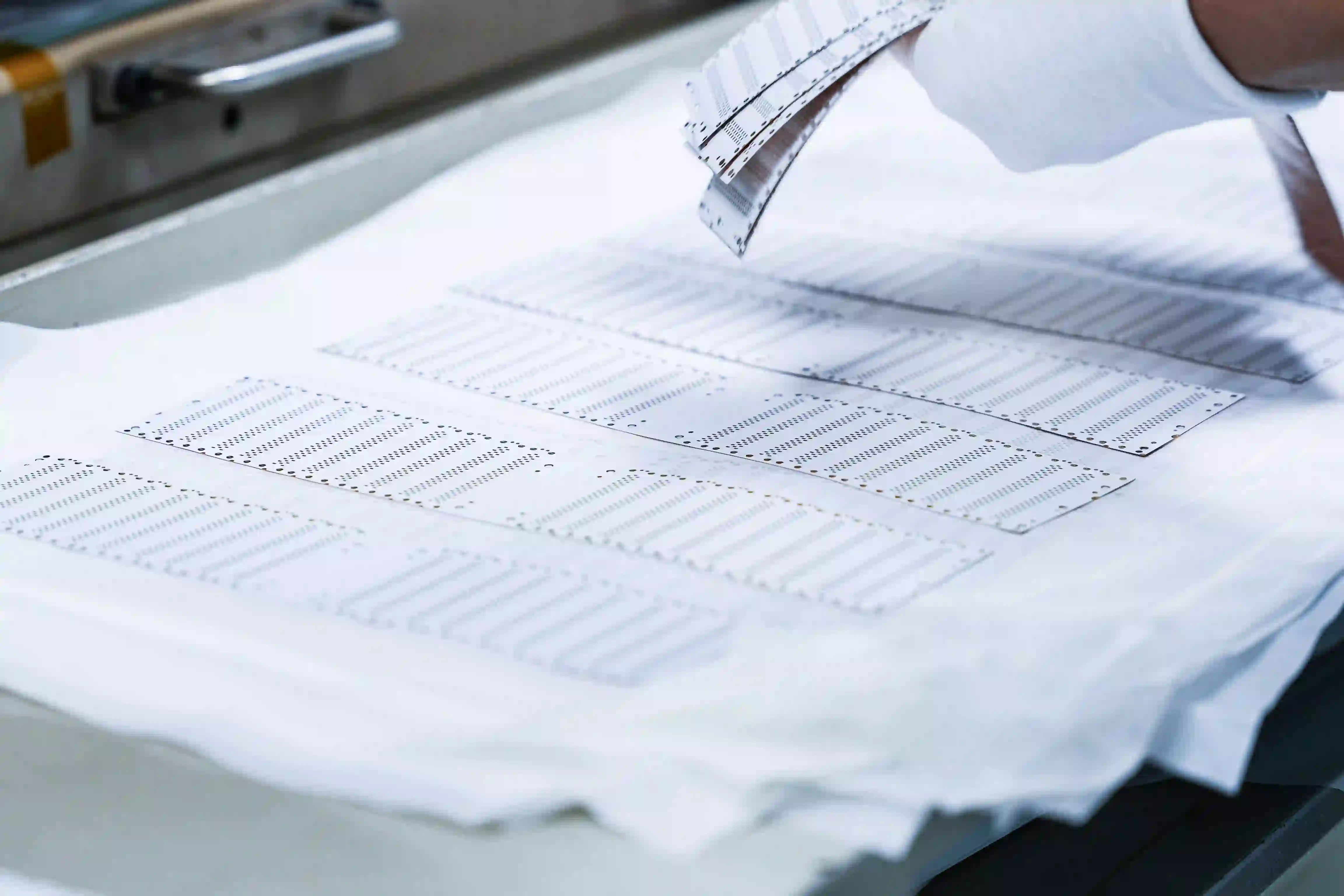
Cold-press the coverlay to eliminate trapped air and ensure intimate contact, then bake under controlled temperature and time to fully cure the adhesive. Proper cure locks dimensions and prevents later delamination during flexing or thermal cycling.
Step 9: Plasma Surface Preparation
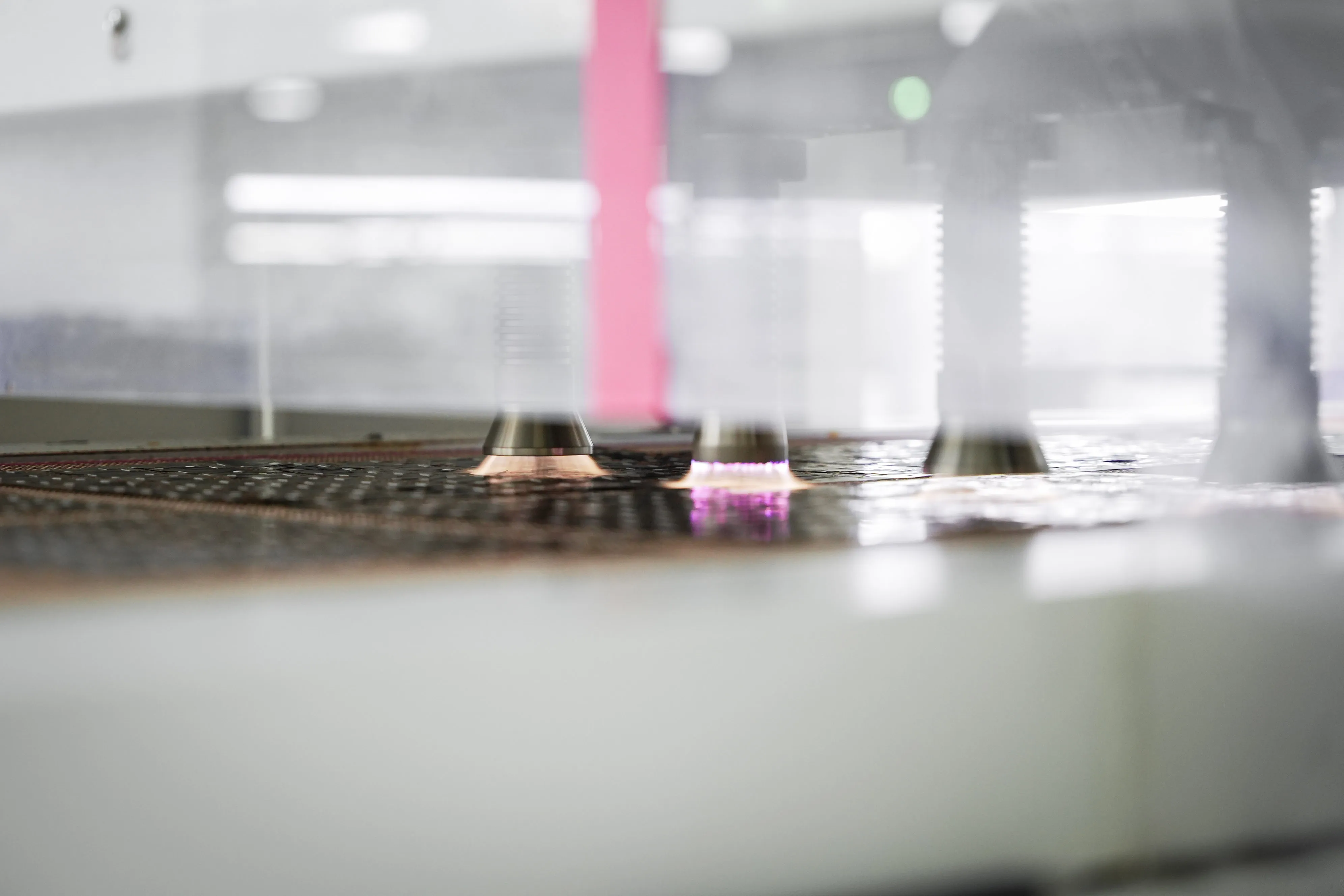
Perform chemical cleaning followed by plasma treatment, which commonly use box-type plasma. This step removes residues and activates the polyimide surface, significantly improving adhesion of subsequent photosensitive ink or other coatings.
Step 10: Photosensitive Solder Mask Coating
Apply photosensitive ink to the required side(s) of the panel. Coating thickness and uniformity are controlled to provide adequate protection without adding excessive stiffness.
Step 11: Solder Mask Exposure and Development
Expose the photosensitive ink through the solder-mask artwork and develop away the unwanted areas, opening the pads and other features.
Step 12: Solder Mask Curing
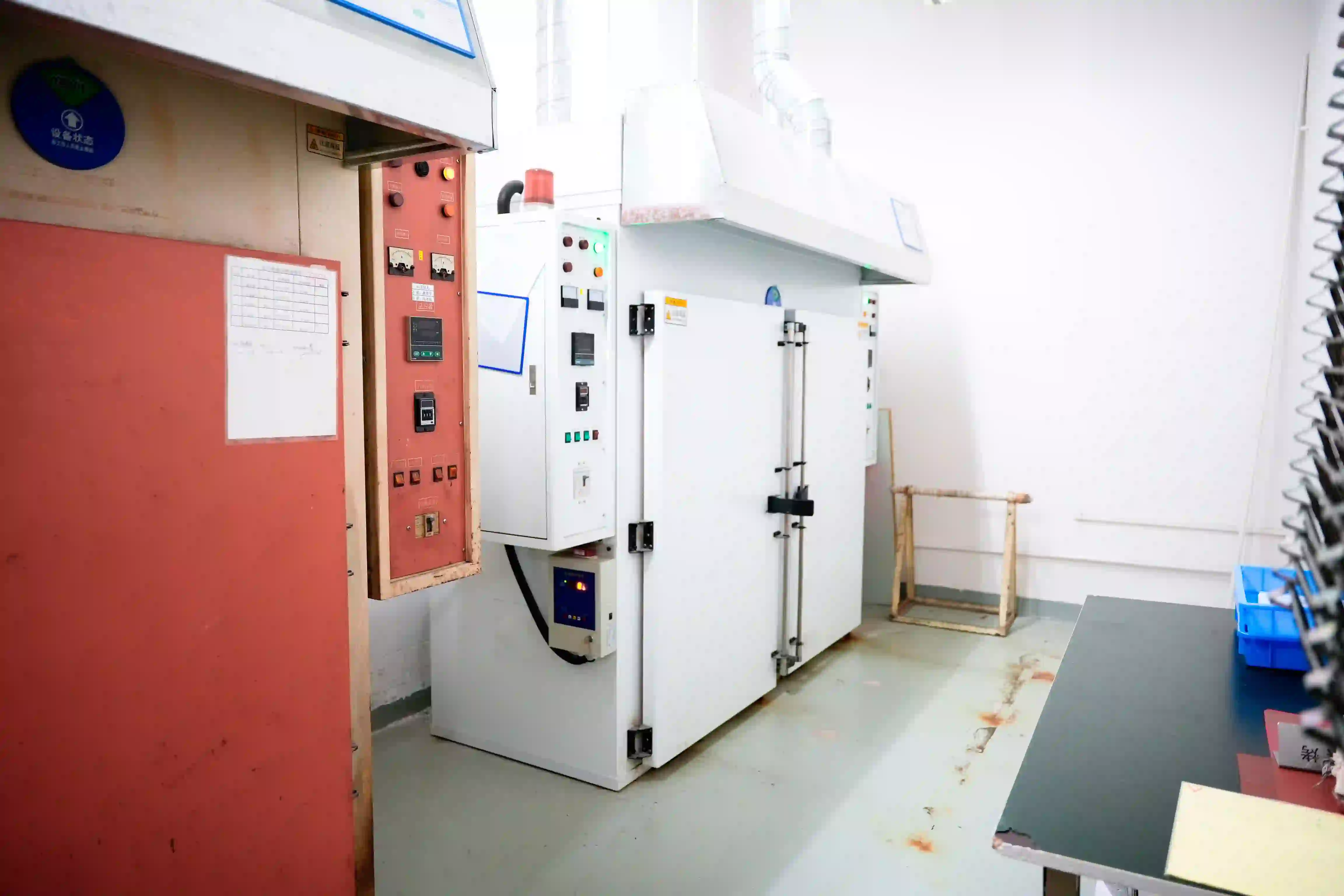
Bake the developed ink under controlled temperature and time to achieve full cure. Incomplete cure leads to ink peeling, blistering, or contamination in later processes.
Step 13: Surface Finish
Apply the specified FPC surface finish (ENIG, OSP, immersion silver, or others) to the exposed copper pads. The finish must provide good solderability or contact reliability while remaining compatible with the intended flex life of the circuit.
Step 14: Electrical Testing
Perform continuity and isolation testing with a dedicated fixture or flying-probe system. This step catches opens, shorts, and high-resistance defects before further value is added.
Step 15: Silkscreen Printing
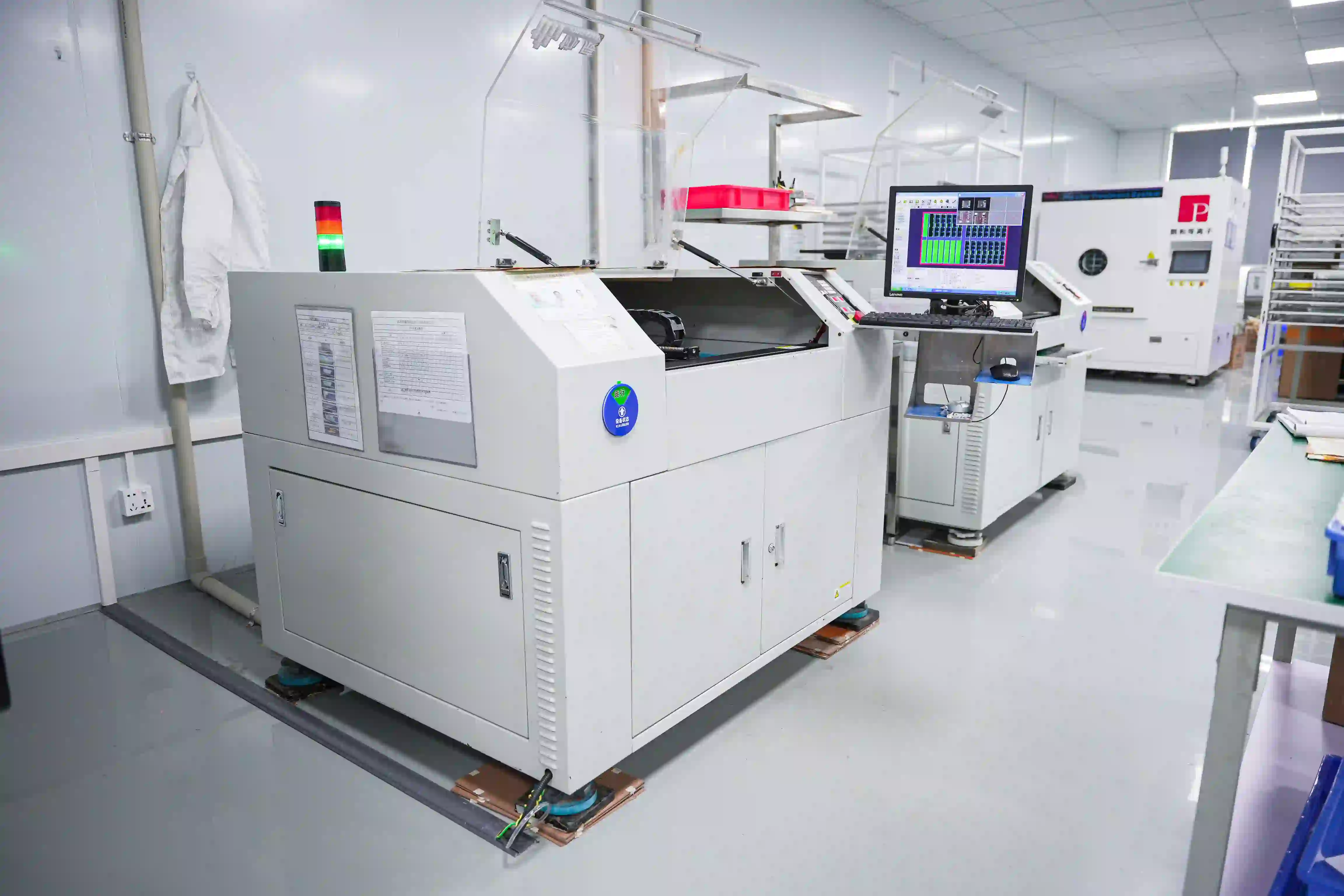
Print identification characters or logos (commonly by silkscreen or jet printing) and cure the ink. Placement and adhesion must survive subsequent handling and FPC assembly.
Step 16: Outline Formation and Singulation
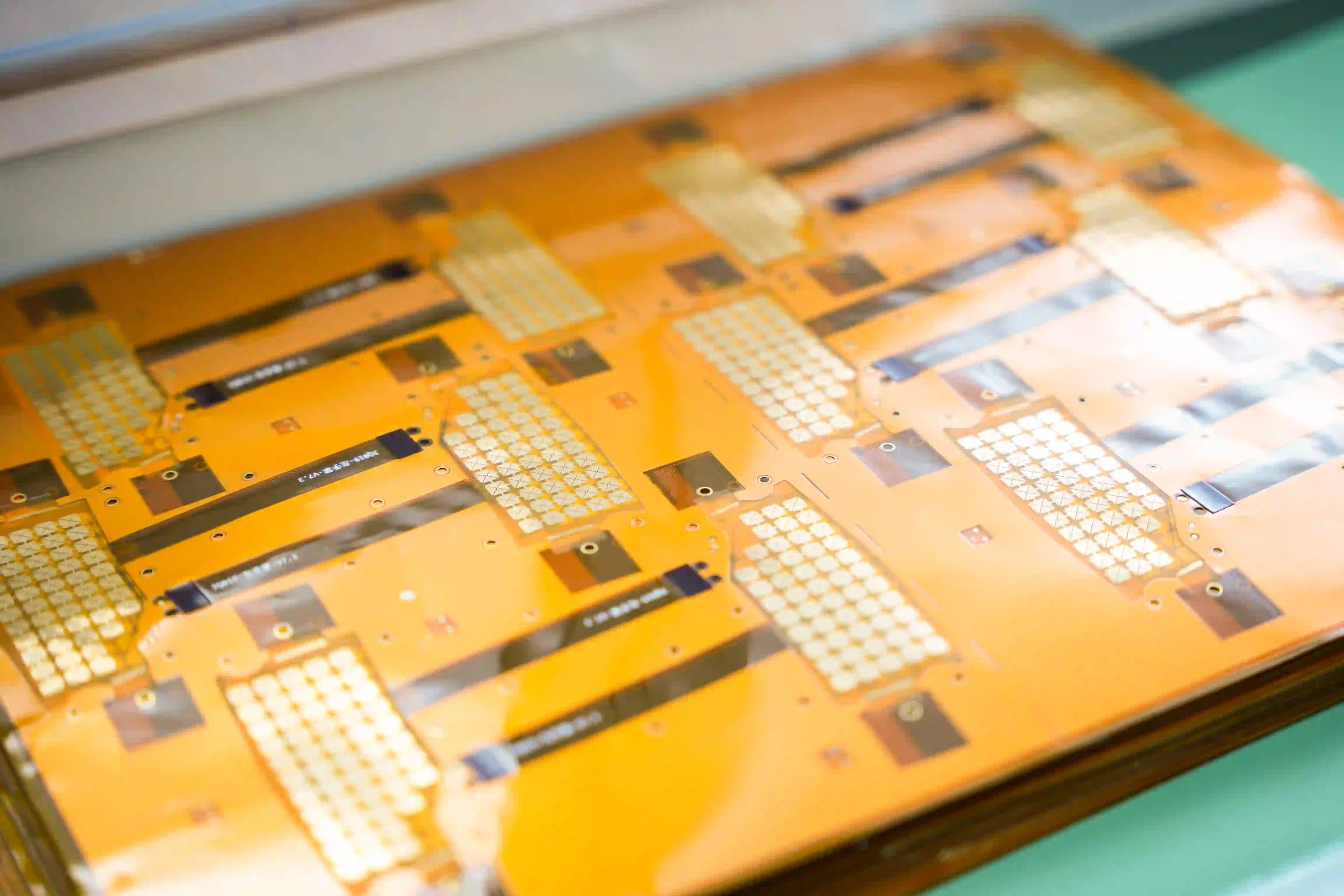
Separate individual circuits from the panel by punching, laser cutting, or a combination of both. Thin flexible material is sensitive to mechanical stress, so tooling and process parameters are chosen to avoid deformation or edge damage.
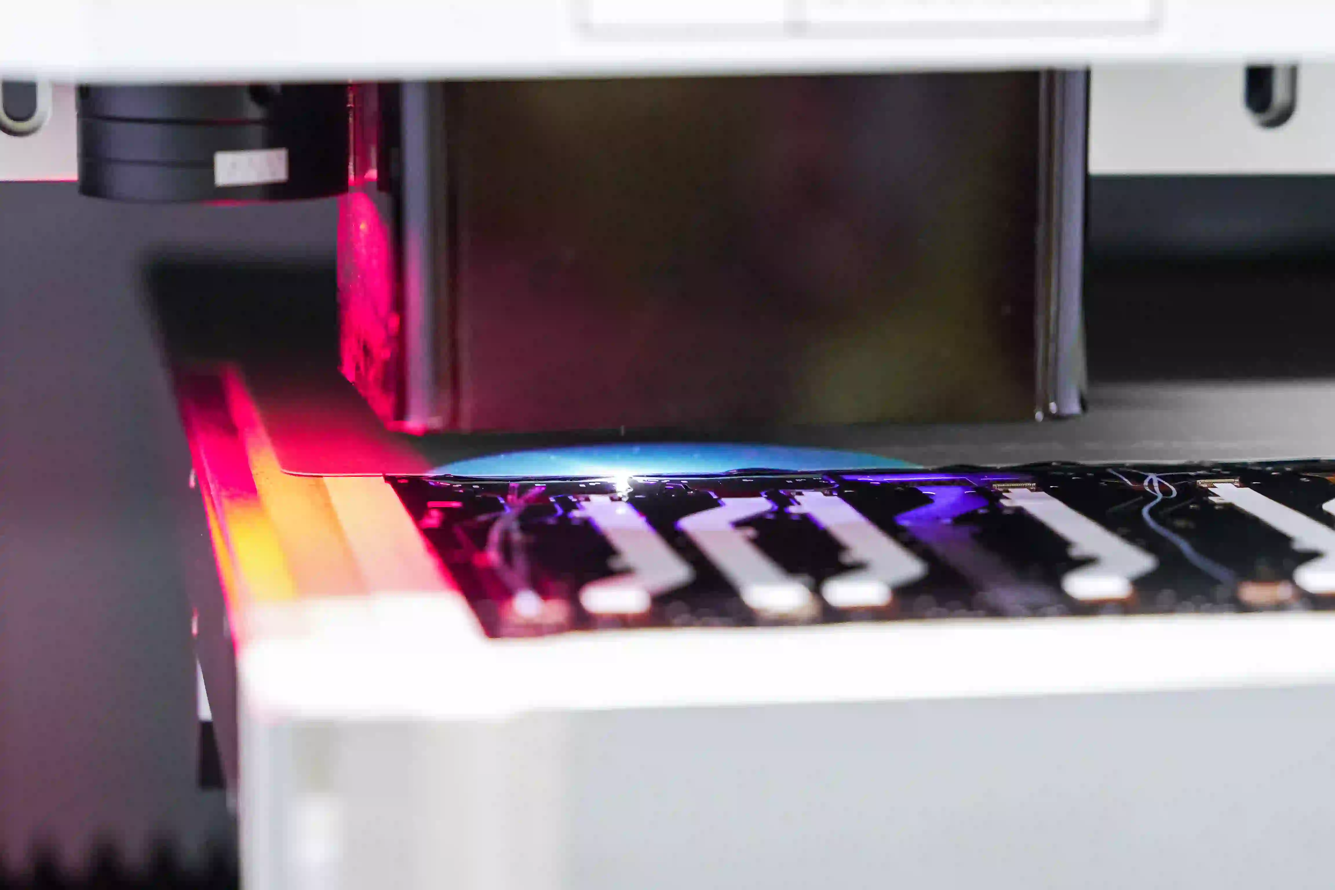
Step 17: FPC Stiffener Attachment
Align and attach local stiffeners where mechanical reinforcement is required. Accurate placement relative to the outline and bend areas is critical for both assembly and long-term reliability.
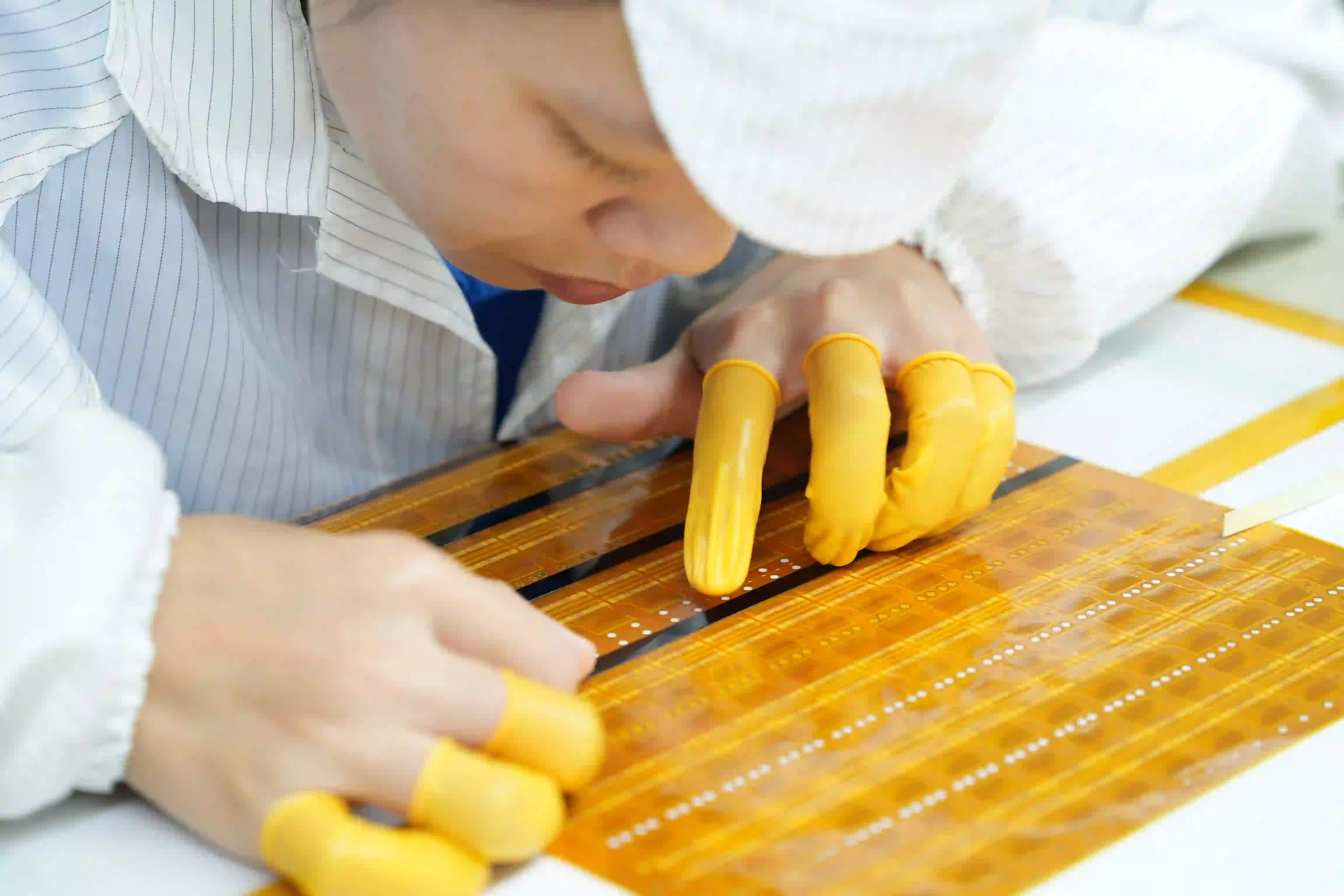
Step 18: Stiffener Pressing and Curing
Press the stiffeners to ensure full contact and bake under controlled conditions to cure the adhesive. This thermal cycle must be managed carefully because the thin FPC has already undergone multiple previous bakes; residual stress at this stage can cause bow or reduced flex life.
Step 19: Final Cleaning and Protective Film Application
Clean the finished circuits and apply protective dust film or release film over sensitive areas (for example, microphone holes or contact pads) to prevent contamination during handling and shipping.
Step 20: Final Quality Control (FQC)
Perform comprehensive final FPC manufaturing inspection covering appearance, dimensions, thickness, electrical performance, and any required reliability sampling (such as bend testing). Only circuits that pass FQC proceed to packaging.
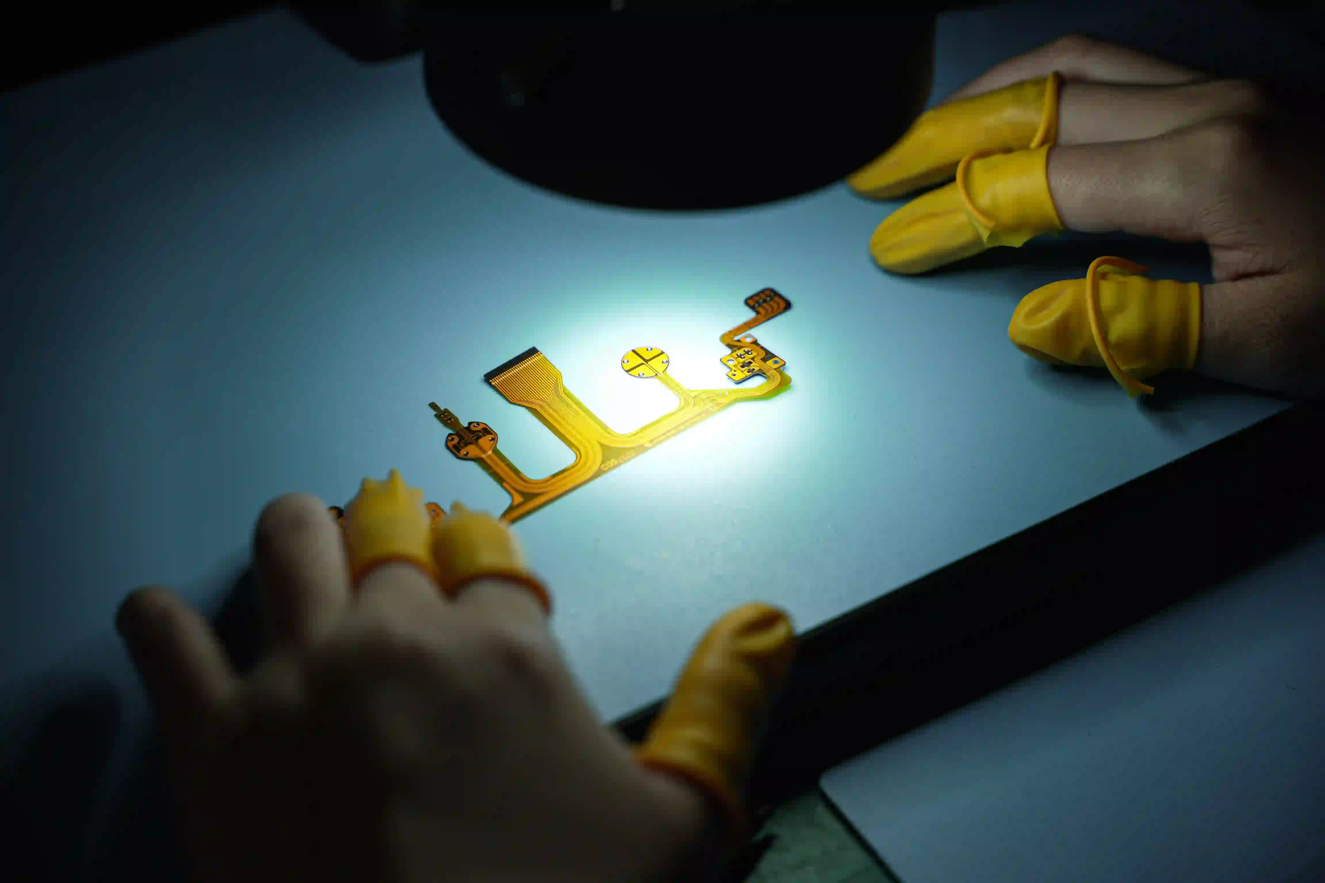
Step 21: Packaging
Package the flexible circuits according to customer or internal requirements, protecting them from moisture, dust, and mechanical damage during storage and transport.
This sequence gives a clear, production-realistic map of single-sided and double-sided FPC manufacturing. Each step exists to control a specific risk, such as dimensional stability, adhesion, copper thickness, surface cleanliness, or mechanical reinforcement. Understanding the order and purpose of these steps allows designers to write better DFM notes and allows buyers to ask the right capability questions when evaluating suppliers.
Key Differences Between Rigid PCB vs FPC Manufacturing Process
Most manufacturing stages, including drilling, imaging, etching, plating, surface finishing, and electrical testing, are shared between rigid and flexible PCB production. The difference lies not in replacing these processes, but in adapting them to thin, flexible polyimide materials with much tighter control over dimensional stability, adhesion, and mechanical reliability.
These additional steps protect the circuit during repeated bending while maintaining precise alignment throughout multiple thermal cycles.
|
Specialized FPC Process |
Why It Is Needed |
|---|---|
|
Coverlay Lamination |
Laminates a polyimide coverlay to protect copper traces while maintaining flexibility. |
|
Multiple Curing Cycles |
Independently cures coverlay, solder mask, and stiffener adhesives for reliable bonding. |
|
Plasma Surface Treatment |
Activates the polyimide surface to improve ink and coating adhesion. |
|
Stiffener Bonding |
Adds localized mechanical reinforcement using FR4, PI, or stainless steel stiffeners. |
|
Punching/Laser Singulation |
Minimizes mechanical stress when separating thin flexible circuits. |
|
Flex Reliability Testing (application dependent) |
Evaluates bend-life performance in products requiring repeated flexing. |
These differences explain why FPC lead times and unit costs are higher. A supplier that runs FPC on the same equipment and parameters used for rigid boards will struggle with registration, coverlay voids, and stiffener adhesion.
Critical Process Control in FPC Manufacturing
Although every FPC manufacturing process stage contributes to product quality, several process nodes have a much greater influence on yield, reliability, and long-term performance. The following sections explain how AIVON controls these critical operations.
Circuit Formation and Fine-Line Control
LDI exposure on thin polyimide demands careful compensation for material movement. The difference between pre- and post-compensation line width/space is normal and must be validated on every new material lot. Etching chemistry and undercut ratio directly determine whether the finished trace can survive repeated flexing.
Coverlay and Multiple Thermal Cycles
Coverlay is usually applied after etching. Cold press ensures no trapped air; the subsequent 160 °C bake cures the adhesive without excessive dimensional shift. Additional baking steps after ink and after stiffener are required because each polymer layer has its own cure profile. Skipping or shortening any bake is a frequent source of later delamination or residual stress.
Hole Metallization
Black-hole plus VCP is the common route for through-holes on single/double-sided FPC. Maintaining 8–12 µm copper thickness balances electrical performance with the need to keep the finished circuit flexible. Thicker copper increases stiffness and reduces bend life.
Surface Finish and Stiffener
ENIG remains the most widely specified finish for soldering reliability. Nickel and gold thickness must stay inside the stated windows; excess nickel can embrittle the circuit under dynamic flex. Steel stiffeners are attached late in the process so that the thin FPC is fully defined before local reinforcement is added. Final thickness after stiffener is a hard customer specification and must be measured on every lot.
Plasma and Surface Preparation
Box-type plasma after chemical cleaning dramatically improves adhesion of photosensitive ink and reduces the risk of ink peeling or blistering during later thermal cycles.
Why Choose AIVON for FPC Manufacturing?
AIVON provides FPC manufacturing support from engineering review through fabrication and final inspection. The production process is designed to accommodate different flexible circuit structures, material configurations, layer counts, and application requirements.
For precision FPC manufacturing for electronics, engineering control is particularly important. AIVON evaluates factors such as material selection, line width and spacing, hole structure, coverlay design, surface finish, stiffeners, and manufacturing tolerances before production.
The manufacturing process can include automated inspection, electrical testing, precision laser processing, and other quality-control procedures according to the requirements of the FPC design. DFM review also helps identify potential manufacturing issues before production begins, allowing the design and manufacturing process to be aligned more effectively.
For projects with specific FPC requirements, customers can submit their design for an engineering review and receive a manufacturing quotation based on the actual board structure and production requirements.
Conclusion
A practical understanding of the FPC manufacturing process flow is essential for reliable design, accurate supplier evaluation, and cost control. The critical windows for hole copper, post-compensation line geometry, coverlay and stiffener cure, and final thickness directly determine both yield and long-term flex performance.
Use this process map when requesting quotes, writing specifications, or auditing a supplier. It turns generic capability claims into concrete questions about plasma systems, bake profiles, compensation values, and thickness control after stiffener. When those questions are answered clearly, the finished flexible circuit is far more likely to meet both the electrical and mechanical requirements of the application.
Related topics on material selection, detailed design rules, and reliability testing will further strengthen the same process-based approach.
FAQ
Q1: What is the most critical process step for yield on thin FPC?
A1: Coverlay application, together with the subsequent cold-press and bake cycle, and precise hole-copper thickness control, typically has the greatest impact on yield. Registration drift after thermal processing is one of the most common causes of downstream failures.
Q2: Why does FPC production take longer than a rigid board of similar complexity?
A2: FPC manufacturing requires multiple low-temperature bake cycles, plasma treatment, coverlay and stiffener lamination, and much gentler material handling than rigid PCB production. These additional process steps increase the overall manufacturing time.
Q3: What surface finishes are compatible with high-flex applications?
A3: ENIG is widely used when reliable solderability is required. OSP preserves maximum flexibility but offers a shorter shelf life. Nickel thickness in ENIG should be carefully controlled to avoid embrittlement in high-flex applications.
Q4: How is dimensional stability controlled throughout the process?
A4: Dimensional stability is maintained by baking materials to remove moisture, controlling tension during handling, curing each polymer layer under a controlled 160 ± 5 °C profile, and verifying registration after every major thermal process. Final board thickness, including stiffeners, is also inspected for every production lot.
Q5: What is the minimum trace width and spacing for a double-layer flexible PCB?
A5: AIVON can achieve a minimum trace width and spacing of 40/40 μm on double-layer FPCs with 8–14 μm surface copper thickness. For more detailed specifications, please refer to our FPC manufacturing capability page.
Q6: What factors affect FPC manufacturing cost?
A6: FPC manufacturing cost is influenced by factors such as material selection, layer count, copper thickness, circuit density, board dimensions, hole technology, coverlay construction, surface finish, stiffeners, testing requirements, and order volume. More complex designs generally require additional processing and tighter manufacturing controls, which can increase production costs.
Q7: How long does FPC manufacturing take?
A7: FPC manufacturing lead time depends on the design complexity, material availability, production quantity, manufacturing process, and testing requirements. Prototype orders are typically handled differently from high-volume production, while multilayer, fine-line, or highly customized FPCs may require additional engineering and production time.
Q8: What materials are commonly used for FPCs?
A8: Polyimide is one of the most widely used substrate materials for FPCs because of its flexibility, thermal resistance, and dimensional stability. Other material choices can include different copper foils, adhesive systems, coverlay materials, and stiffeners, depending on the electrical, mechanical, and environmental requirements of the application.
Q9: What is the minimum bend radius of an FPC?
A9: The minimum bend radius depends on the FPC thickness, copper type, layer count, material construction, and whether the circuit is designed for static or dynamic bending. A circuit intended for repeated flexing generally requires a larger bend radius and a design that minimizes stress on copper traces and other interfaces.
Q10: Can FPCs be manufactured with components?
A10: Yes. FPCs can be combined with electronic components through processes such as SMT assembly. However, component placement needs to consider the flexible area's bending behavior, component size, pad design, stiffener requirements, and assembly conditions. Components are often positioned in areas where sufficient mechanical support is available.
Q11: What is the difference between FPC and FFC?
A11: FPC and FFC are both flexible interconnection solutions, but their structures and manufacturing methods are different. FPCs use patterned copper circuitry and can support more complex routing, multilayer structures, and customized geometries. FFCs generally use parallel conductors within a flat flexible cable structure and are commonly used for simpler point-to-point connections.
Q12: What design files are needed for FPC manufacturing?
A12: Manufacturers typically require design data such as Gerber or other supported fabrication files, drill information, layer specifications, material requirements, and relevant production notes. For more complex FPC projects, a BOM, assembly data, stack-up information, and mechanical drawings may also be needed.
Q13: What are common FPC manufacturing defects?
A13: Common FPC defects can include trace width variation, open or short circuits, hole defects, coverlay misalignment, delamination, scratches, surface contamination, dimensional deviation, and stiffener misalignment. The actual defect risks depend on the FPC structure, materials, design tolerances, and manufacturing requirements.
Q14: How can an FPC design be optimized for manufacturing?
A14: An FPC can be made more manufacturing-friendly by selecting appropriate materials, maintaining realistic trace and spacing requirements, providing suitable bend areas, avoiding unnecessary sharp corners, defining appropriate tolerances, and considering coverlay, stiffener, hole, and assembly requirements during the design stage. Early DFM review can help identify potential manufacturing issues before fabrication.
Q15: Is FPC suitable for high-volume production?
A15: FPCs can be manufactured for both prototype and high-volume applications. The appropriate production approach depends on circuit complexity, material construction, order volume, dimensional requirements, and manufacturing technology. High-volume production may benefit from process standardization and production methods suited to continuous or repeat manufacturing.