When a flexible PCB fails after a few thousand bend cycles or shows intermittent opens only after SMT, the cost is rarely limited to the board itself. Assembly lines stop, field returns climb, and engineering teams spend weeks chasing root causes that often started months earlier in the manufacturing process.
FPCs are more vulnerable than rigid boards. Thin polyimide, rolled-annealed copper, sensitive coverlay lamination, and the absence of glass reinforcement mean that small process variations turn into opens, delamination, or warpage far more easily. Many of these issues pass initial electrical test and only appear under mechanical or thermal stress.
Highlights
● Most costly FPC field failures trace back to a handful of manufacturing defects that are preventable with proper DFM and process control.
● Copper cracking at bend zones and coverlay-related issues remain the two highest-impact failure modes in dynamic flex applications.
● Combining design rules with tight lamination and inspection controls typically delivers the largest yield gains.
This article walks through the ten highest-impact FPC manufacturing defects, explains how they form, shows practical ways to prevent them, and outlines a workable failure-analysis workflow you can apply the next time a problem appears.
Why FPC Manufacturing Defects Occur More Easily Than Rigid PCBs
Rigid PCBs sit on a stable FR-4 core. Flexible printed circuits do not. Most single- and double-sided FPCs use polyimide films between 12 µm and 50 µm thick. That thin dielectric offers almost no mechanical support once the copper is etched. Rolled-annealed copper, preferred for flex life, still work-hardens under repeated bending. Coverlay must be laminated with precise temperature, pressure, and vacuum; any trapped air or misalignment creates a weak point that grows under stress.
Moisture absorption, CTE mismatch during reflow, and the multiple handling steps required for stiffener attachment and forming add further risk. A defect that would be cosmetic on a rigid board often becomes an electrical open or intermittent connection on an FPC.
The FPC manufacturing process itself creates multiple opportunities for defects: material preparation and baking, imaging and etching, coverlay lamination, stiffener attachment, surface finish, electrical test, and final form or laser punch. Understanding where each defect originates is the first step toward prevention.
The 10 Most Common FPC Manufacturing Defects
These ten defects account for the majority of yield loss and field failures observed in high-volume FPC production. They are grouped by type for clarity.
|
No. |
Common FPC Defects |
|---|---|
|
1 |
Open Circuits and Conductor Fractures |
|
2 |
Short Circuits |
|
3 |
Over-Etching, Under-Etching, Necking, Edge Roughness |
|
4 |
Coverlay Alignment Issues and Incomplete Coverage |
|
5 |
Coverlay Bubbles, Voids, and Delamination |
|
6 |
Substrate Wrinkles, Creases, and Dimensional Deformation |
|
7 |
Pad or Trace Lifting/Peeling |
|
8 |
Copper-Polyimide or Interlayer Delamination |
|
9 |
Warpage, Bow, and Twist |
|
10 |
Surface Damage, Scratches, Dents, and Contamination |
Circuit Pattern Defects in FPC Manufacturing
1. Open circuits and conductor fracture
Appearance: Complete break or fine crack across a trace, often visible only under magnification or after bend testing. In dynamic zones the crack frequently starts at the outer surface of the copper.

Impact: Permanent or intermittent open.
Reason: The primary cause is repeated mechanical stress that exceeds the fatigue limit of the copper, especially when the bend radius is too tight or traces run perpendicular to the bend axis. Secondary contributors include the use of electrodeposited copper in dynamic applications, localized thinning from over-etching, and edge damage introduced during punching or laser cutting. These factors create micro-cracks that grow under cyclic flexing until the conductor fully opens.
Detection: Flying-probe or fixture test may catch gross opens; micro-cracks often appear only after bend-cycle or thermal-shock testing, or in the field.
2. Short circuits
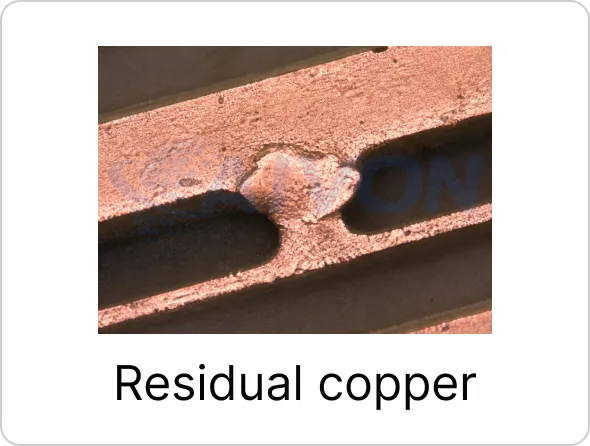
Appearance: Residual copper bridges, conductive particles, or incomplete etching between adjacent traces or pads.
Impact: Functional failure or component damage.
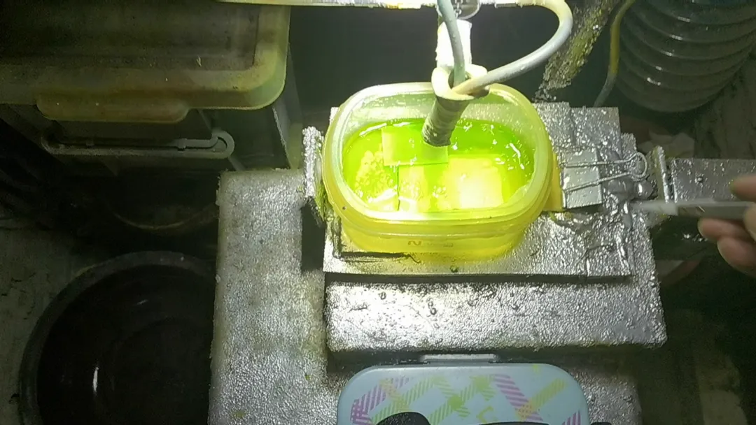
Reason: The most common root cause is incomplete etching caused by photoresist defects such as pinholes or residual resist that protects unwanted copper. Process chemistry imbalance and insufficient agitation can leave residual copper between fine spaces. Conductive particles from copper powder, tin beads, or environmental contamination that become trapped under the coverlay also create bridges that pass initial visual checks but fail electrically.
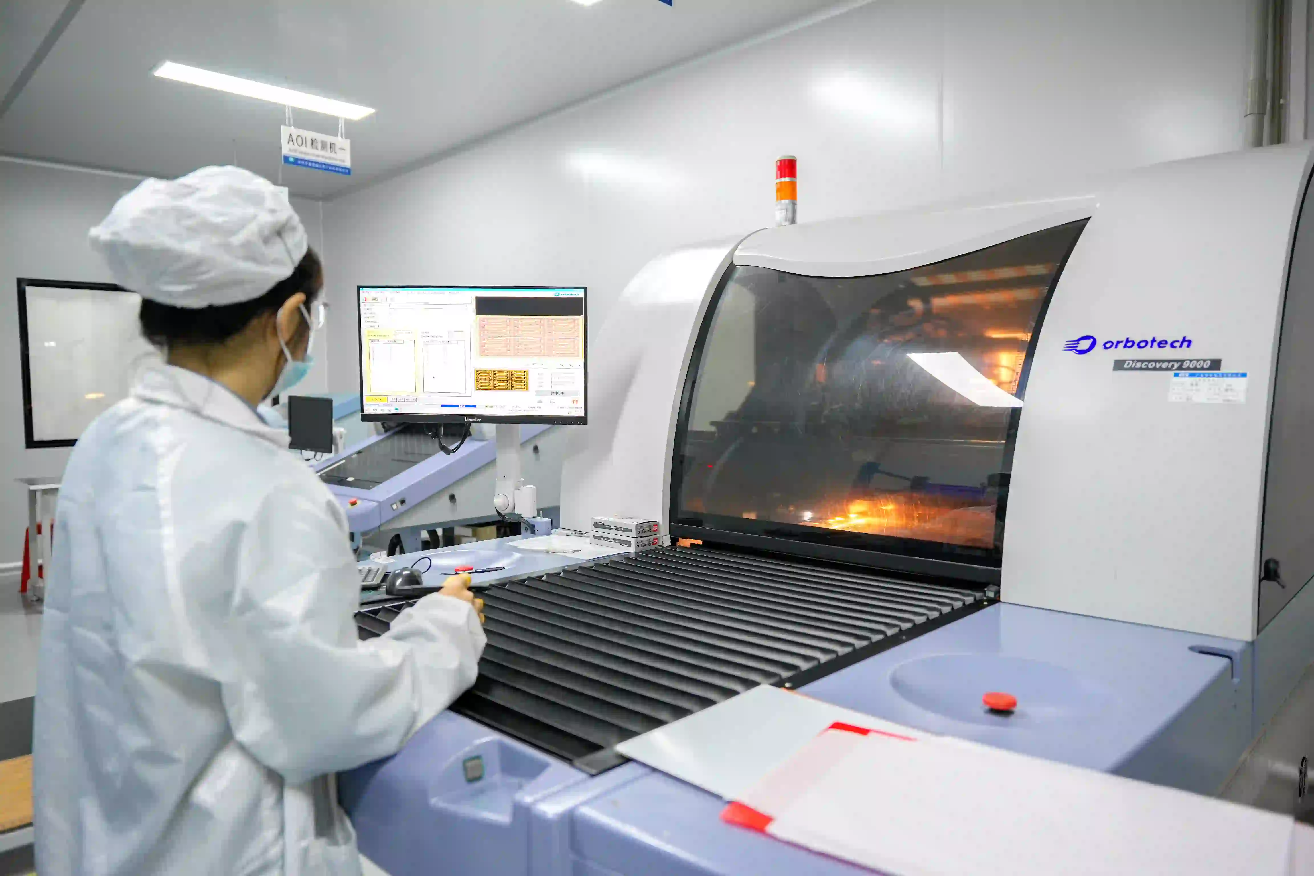
Detection: Usually caught by electrical test; fine bridges may require AOI or magnified visual inspection.
3. Over-etching, under-etching, necking, and edge roughness
Appearance: Traces thinner than designed, uneven sidewalls, residual copper in spaces, or localized necking.
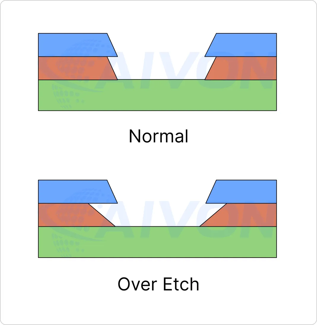
Impact: Reduced current-carrying capacity, higher resistance, or stress-concentration points that later crack.
Reason: Etch process instability is the dominant factor. Variations in etchant concentration, temperature, or dwell time produce uneven copper removal, leading to necking or residual copper. Uneven photoresist coverage and incoming copper thickness variation amplify the problem, creating stress risers that later become crack initiation sites under mechanical load.
Detection: AOI and dimensional measurement; sometimes only after electrical performance testing.
Coverlay and Base Material Defects in Flexible PCBs
4. Coverlay misalignment or incomplete coverage
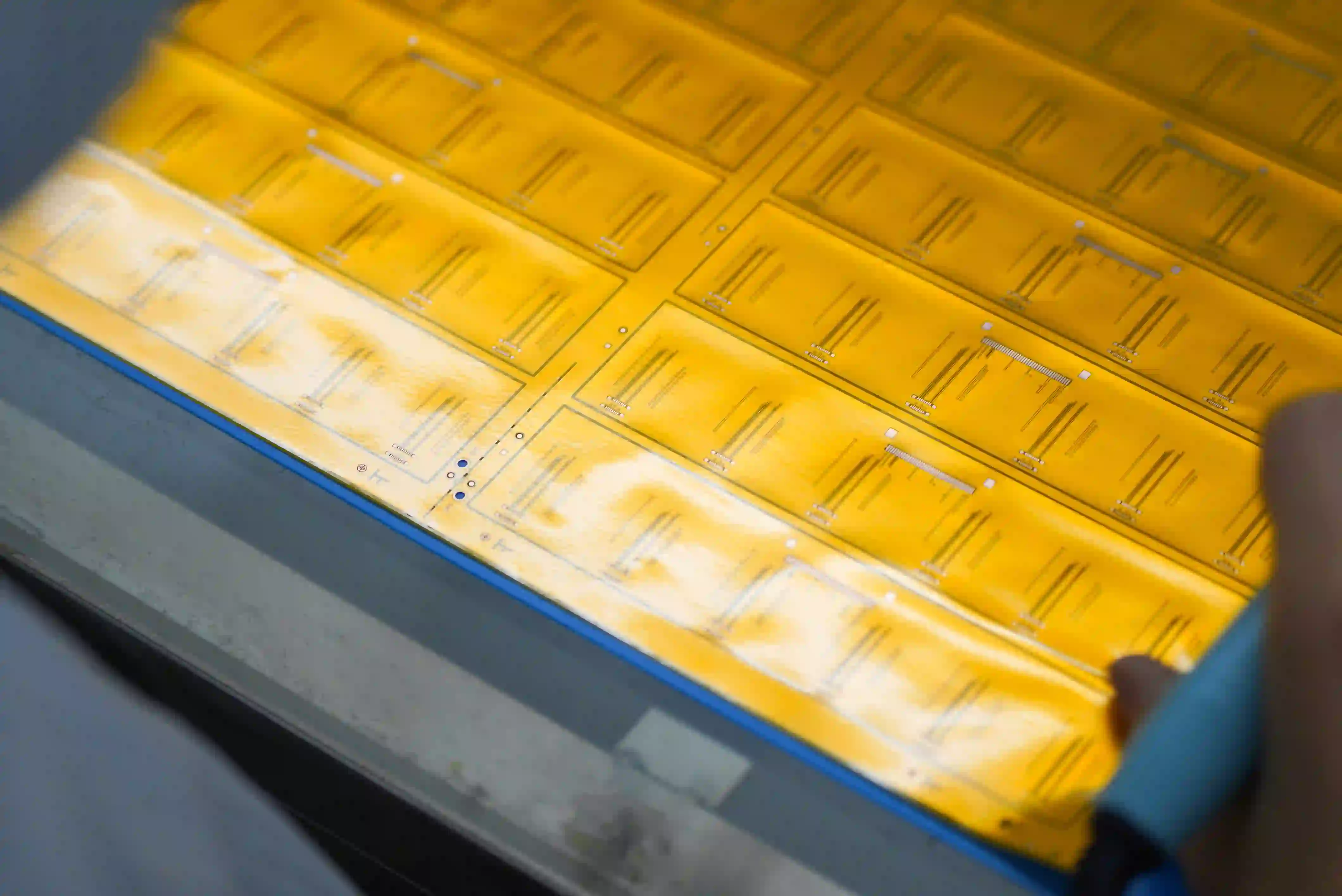
Appearance: Flex PCB coverlay shifted relative to pads or traces, leaving copper exposed or covering areas that should remain open.
Impact: Oxidation risk, shorting, or inability to solder.
Reason: Alignment accuracy of the coverlay placement equipment or tooling is the leading cause. Panel dimensional change after earlier processes (such as etching or baking) and operator setup variation further increase the chance of shift. When the coverlay is even slightly offset, critical pads or traces become either exposed or covered, directly affecting solderability and long-term reliability.
Detection: Visual or AOI after lamination.
5. Coverlay bubbles, voids, and delamination
Appearance: Local unbonded areas, raised blisters, or edge lifting.
Impact: Moisture ingress, reduced dielectric strength, and progressive separation under flexing.
Reason: Inadequate lamination parameters, particularly insufficient vacuum, incorrect temperature ramp, or improper pressure, are the primary drivers. Residual moisture in the polyimide or adhesive, surface contamination, and marginal adhesive quality prevent full wetting and bond formation. The resulting voids act as stress concentrators and pathways for moisture, allowing the defect to grow during subsequent thermal or mechanical stress.
Detection: Visual inspection, AOI, or cross-section; latent voids may only appear after reflow or humidity exposure.
6. Substrate wrinkles, creases, or dimensional distortion
Appearance: Wavy surface, permanent crease lines, or overall panel shrinkage/expansion outside tolerance.
Impact: Registration errors in later steps, assembly fit problems, and stress concentration.
Reason: Uneven tension control during material handling and lamination is the main contributor. Moisture absorption by the polyimide followed by rapid drying or temperature change causes differential shrinkage. Improper stacking, storage, or roller pressure during processing permanently deforms the thin substrate, locking in wrinkles and dimensional errors that affect downstream registration.
Detection: Visual and dimensional measurement after lamination or forming.
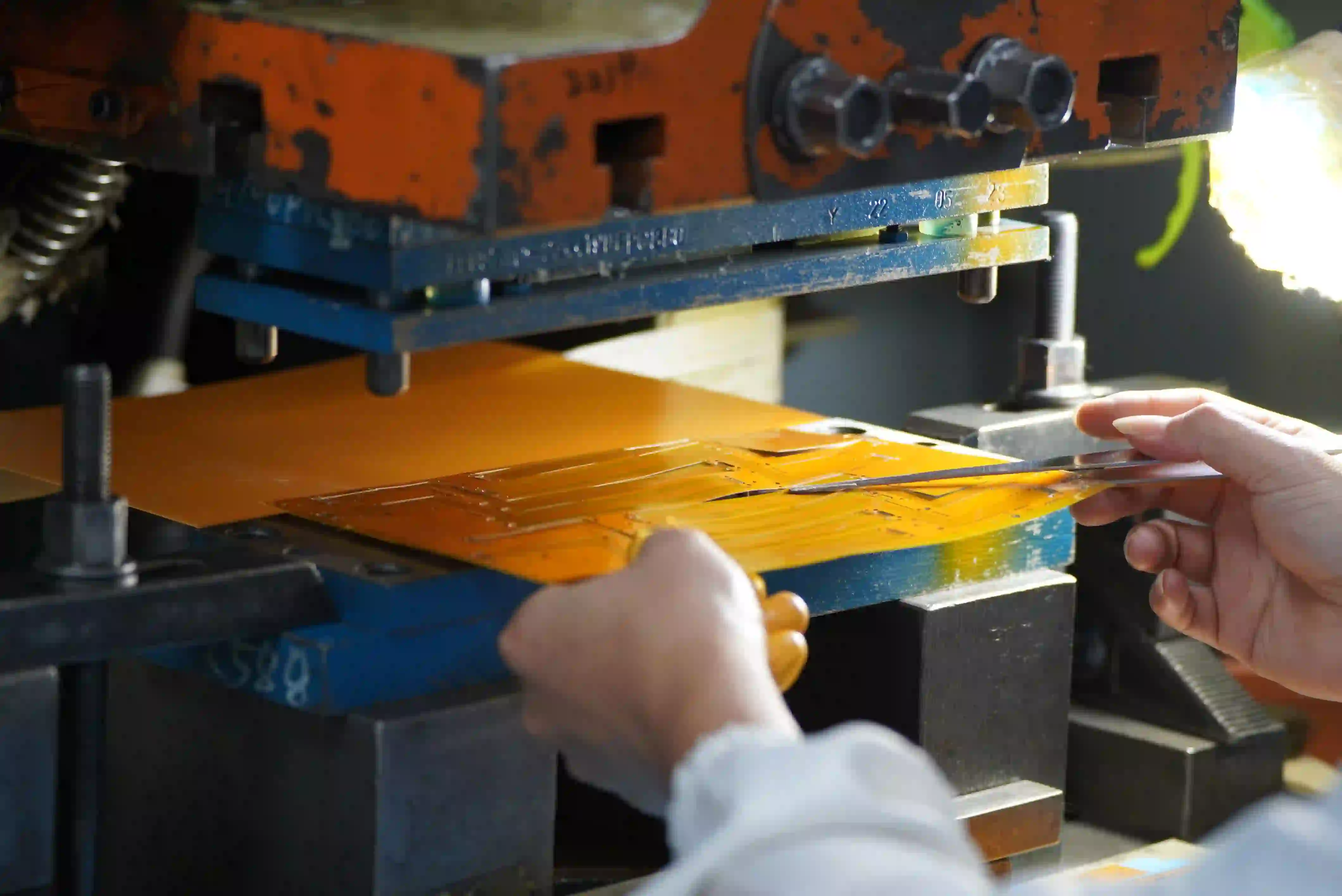
Mechanical and Structural Defects in Flexible PCB Manufacturing
7. Pad or trace lifting/peeling
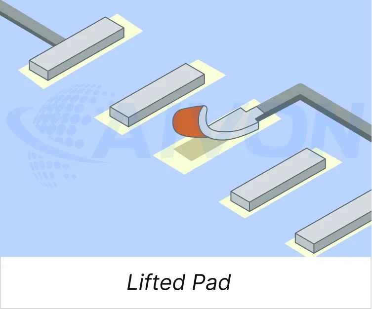
Appearance: Copper separating from the polyimide, especially around pads after soldering or rework.
Impact: Open circuits and assembly scrap.
Reason: Insufficient copper-to-polyimide adhesion is the dominant root cause. Excessive heat or mechanical force applied during soldering or rework then peels the already weakly bonded copper. Incomplete surface preparation before plating or coverlay application further weakens the interface, making pads especially vulnerable under thermal and mechanical load.
Detection: Visual after soldering or mechanical peel testing.
8. Delamination between copper and polyimide or between layers
Appearance: Layer separation visible as blisters or edge lifting; may be internal and only visible in cross-section.

Impact: Loss of mechanical integrity and eventual electrical failure.
Reason: Residual moisture that turns into vapor during reflow is the most frequent trigger. Weak adhesive bonds resulting from suboptimal lamination parameters and CTE mismatch between copper, polyimide, and adhesive layers allow the vapor pressure to separate the interfaces. Contamination at the bonding surface accelerates the process and reduces the margin against thermal stress.
Detection: Visual, thermal stress testing, or micro-section.
9. Warpage, bow, and twist
Appearance: Panel or individual circuit that does not lie flat, especially on ultra-thin or asymmetrically covered constructions.
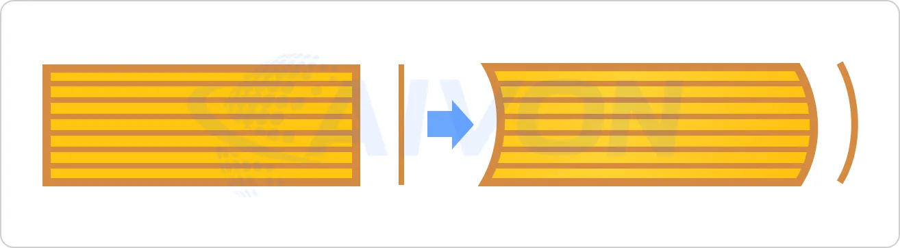
Impact: Placement errors during SMT, poor connector contact, and handling damage.
Reason: Unbalanced material distribution, particularly asymmetric copper or coverlay coverage, is the primary cause on thin constructions. Residual stress locked in during lamination and curing, combined with the inherently low stiffness of ultra-thin polyimide, produces bow and twist. Lack of temporary process-edge stiffening further allows the panel to deform during subsequent handling and thermal cycles.
Detection: Visual flatness check or measurement against a reference surface.
Surface Damage and Handling Defects
10. Scratches, dents, mechanical damage, and contamination
Appearance: Surface marks, compressed copper, foreign particles, or fingerprints.
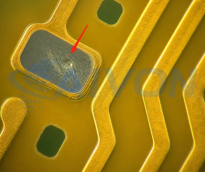
Impact: Opens, shorts, or reduced insulation resistance.
Reason: Improper handling and stacking of the thin, flexible panels is the leading source of mechanical damage. Worn rollers, tooling, or release films introduce dents and scratches, while inadequate clean-room discipline allows particles and fingerprints to contaminate the surface. These defects may be latent and only become electrically significant after later processing or environmental exposure.
Detection: Visual or AOI; some contamination only appears after electrical or environmental testing.
How to Prevent Common FPC Manufacturing Defects
Prevention is far more effective than detection. The highest leverage comes from combining DFM rules with disciplined process windows and targeted inspection.
Flex PCB Delamination: Causes and Prevention
Flex PCB delamination occurs when the copper, polyimide, coverlay, adhesive, or other bonded layers begin to separate. It can appear as bubbles, edge lifting, blisters, or internal separation that is only visible after cross-sectioning. In some cases, the board may pass initial electrical testing but develop reliability problems after reflow, thermal cycling, humidity exposure, or repeated flexing.
Several manufacturing factors can contribute to flex PCB delamination. Moisture trapped in polyimide or adhesive layers can expand rapidly during reflow and create internal pressure at weak interfaces. Inadequate lamination temperature, pressure, vacuum, or dwell time can also prevent the adhesive from fully flowing and bonding to the copper surface. Contamination between layers, insufficient surface preparation, and CTE differences between copper, polyimide, and adhesive materials can further reduce bond strength.
Prevention starts with controlling the materials before lamination. Polyimide and copper-clad materials should be stored under appropriate conditions and baked when required to reduce moisture-related defects. During lamination, manufacturers should maintain stable temperature, pressure, vacuum, and dwell-time parameters for the selected material stack. Surface cleanliness is equally important because particles or residue between the copper and bonding layer can create localized weak points.
For designs using thick copper or dense copper features, adhesive thickness and resin flow should also be considered. The bonding material must have enough flow capability to fill the spaces around copper features and establish sufficient contact with the surrounding surface. AIVON's FPC production process therefore treats coverlay lamination and material preparation as critical process controls rather than relying only on final inspection.
After lamination, visual inspection, cross-section analysis, peel-strength testing, and thermal or humidity stress testing can help identify latent bonding problems. Combining material control, optimized lamination parameters, clean interfaces, and appropriate inspection reduces the risk of delamination reaching assembly or field use.
DFM Rules to Prevent Flexible PCB Defects
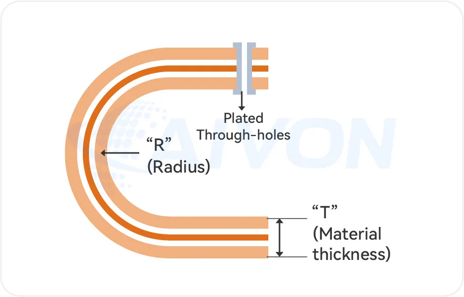
Minimum bend radius remains the single most important design parameter. For static (one-time) bends, a radius of 6× the total flex thickness is a common starting point. For dynamic flexing, 10× or greater is safer; critical high-cycle applications often require even larger radii. Place conductors as close as possible to the neutral axis. Use radiused corners and teardrop transitions at pads. Keep vias out of bend zones. Specify rolled-annealed copper for any circuit expected to flex repeatedly. Design gradual stiffener transitions rather than sharp steps.
A practical checklist used by many fabricators includes:
● Confirm FPC bend radius against total stack thickness and copper type
● Orient critical traces parallel to the bend axis
● Verify coverlay openings provide adequate pad support (typically ≥0.1 mm overlap)
● Check stiffener edge location relative to bend line
● Match copper weight to expected flex life (½ oz or thinner often preferred for dynamic zones)
A Practical Failure Analysis Workflow
When defects appear, a structured approach saves time:
1. Collect complete failure history, ncluding when the failure first appeared, environmental conditions, number of cycles or thermal exposures, and any process changes.
2. Perform visual and low-power microscopic inspection of the failed area and surrounding regions.
3. Conduct non-destructive electrical characterization.
4. If the cause remains unclear, prepare cross-sections and, when needed, SEM/EDX analysis.
5. Correlate findings back to specific design features and process steps.
6. Implement corrective actions and verify on subsequent production or reliability samples.
A frequent pitfall is assuming every open is a manufacturing defect. Assembly handling, incorrect fixtures, or excessive rework heat can produce identical symptoms. Always examine both the board and the assembly process before drawing conclusions.
AIVON Process Controls for Preventing FPC Defects
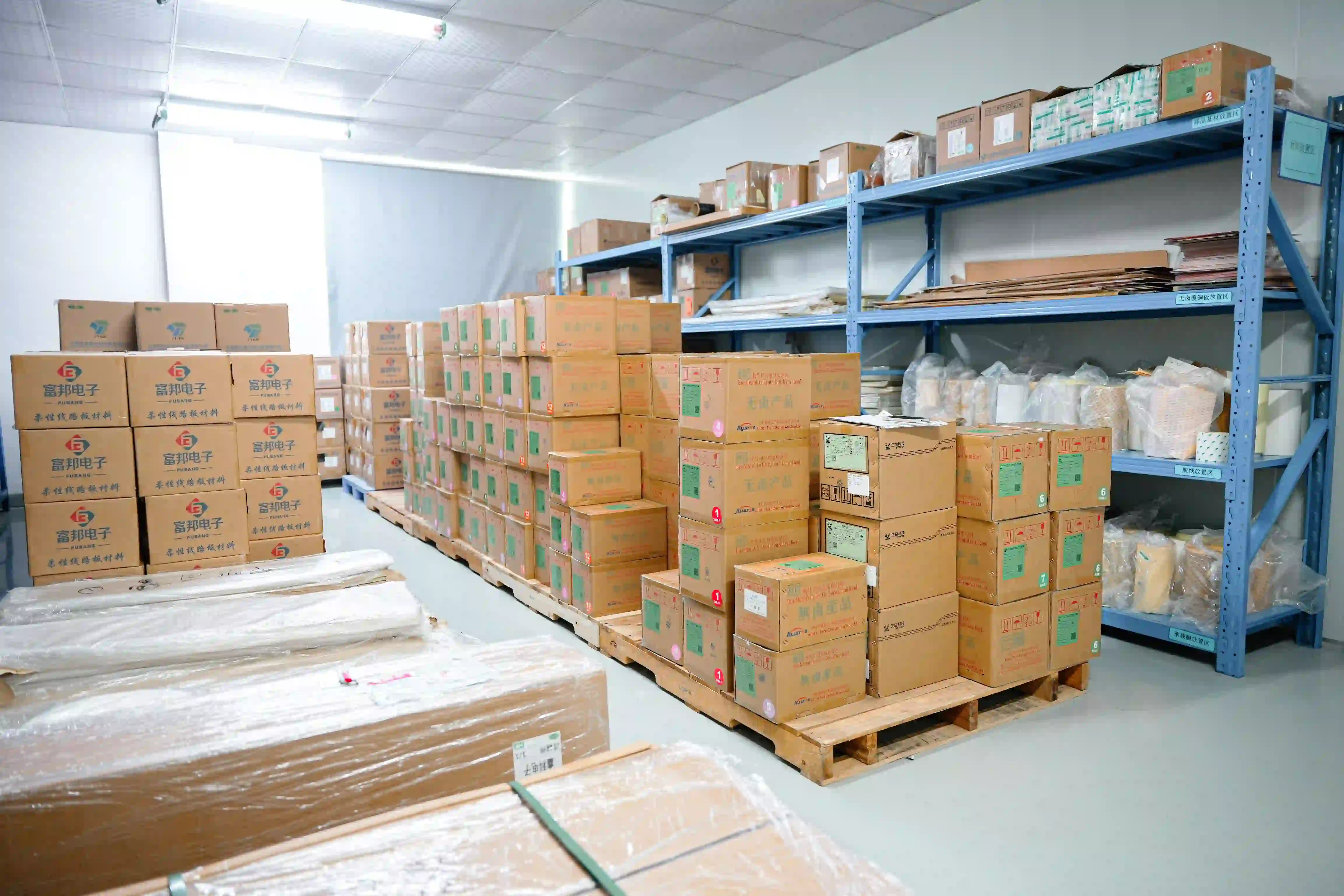
At AIVON, defect prevention begins with strict incoming material control. All polyimide and copper-clad laminates are baked according to supplier specifications and held in controlled-humidity storage until they enter production. This step significantly reduces the risk of moisture-related delamination and dimensional instability later in the process.
Coverlay lamination is treated as a critical process window. Temperature profile, pressure, vacuum level, and dwell time are locked to proven parameters for each material stack. Continuous monitoring ensures that small deviations, which commonly create voids or weak bonds, are caught and corrected in real time. Punching dies and laser systems undergo scheduled wear inspection and preventive maintenance so that edge quality remains consistent and micro-cracks from tooling are minimized.
For customers who perform SMT in-house, AIVON provides recommended reflow profiles tailored to the specific FPC thickness and stack-up. These profiles limit peak temperature and time above liquidus, helping to avoid residual moisture expansion and excessive warpage on ultra-thin circuits.
Inspection Methods for Detecting FPC Manufacturing Defects
In AIVON's actual production flow, comprehensive quality control in FPC manufacturing and key inspection points are built directly into the process sequence rather than relying only on end-of-line screening.
After circuit imaging, etching, and coverlay lamination, key dimensional requirements are verified, including minimum line width/spacing and overall FPC thickness after pressing. These checks confirm that the circuit pattern and stack-up remain within specification before further processing.
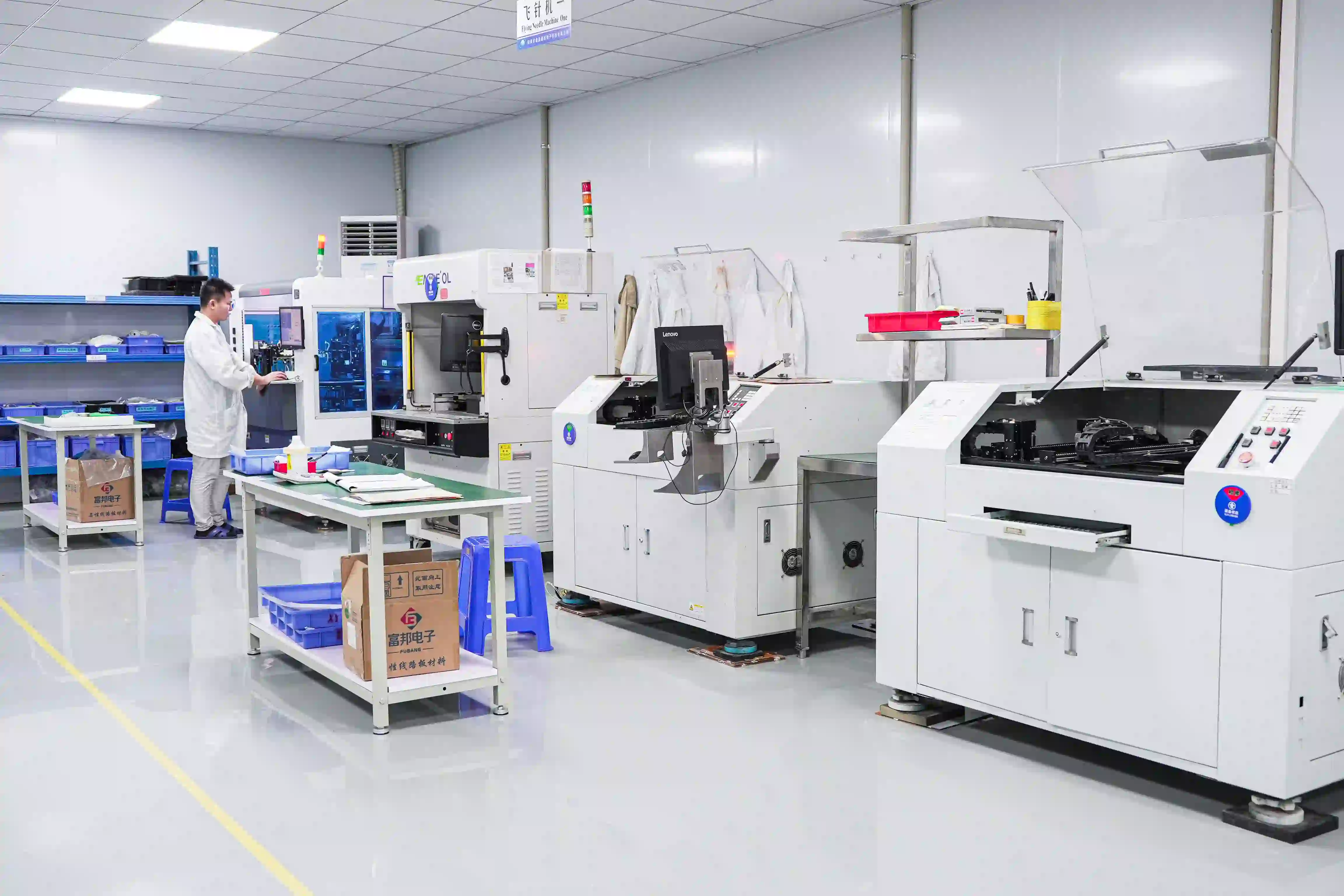
Electrical testing is performed after surface finish (ENIG) using a dedicated test frame. This 100% electrical test screens for opens and shorts before the panels move to mechanical forming.
Following outline punching, steel stiffener attachment, final baking, cleaning, and plasma treatment, every panel undergoes Final Quality Control. FQC includes visual inspection for coverlay integrity, stiffener alignment and adhesion, surface contamination, scratches, and overall appearance. Only panels that pass FQC proceed to in-house SMT or packaging.

This staged approach allows defects to be identified at the point they are most likely to occur, reducing the chance of latent issues reaching the customer.
How AIVON Supports Customer Quality Goals
Rather than simply responding to problems after they appear, AIVON shares process capability data on critical dimensions and detailed control plans for coverlay lamination and etching during the quotation and DFM review stages. Early engineering collaboration allows potential risk points, such as tight bend radii, asymmetric coverlay, or challenging copper weights, to be identified and mitigated before tooling is cut. Factories that routinely provide this level of transparency and engage in joint DFM reviews consistently deliver more stable quality and higher first-pass yields.
Real Manufacturing Cases of Flexible PCB Defects
Case 1: Fine-Line Copper Thickness & Solder Mask Bridge
During the CAM review of a double-sided FPC order, AIVON engineers identified two critical manufacturability risks before any material was issued. On the bottom layer, several pads were spaced too closely to retain reliable solder-mask bridges, which would have created a high risk of solder bridging during assembly. At the same time, the designed trace width and spacing of 0.07/0.07 mm could not support a full 1 oz finished copper thickness without severe over-etching or necking.
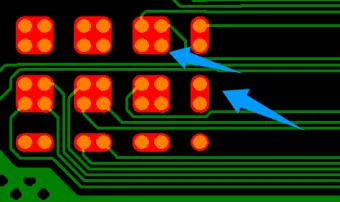
The team recommended opening solder-mask windows on the tight-pitch pads and adjusting the copper thickness targets: inner-layer finished copper to 18 µm (0.5 oz) and outer-layer finished copper to 27 ± 5 µm. These changes were accepted by the customer prior to tooling. As a result, the order avoided potential open-circuit defects from over-etched fine lines and short-circuit risks from missing solder-mask dams, while still meeting the electrical and mechanical requirements of the application.
This type of proactive file review is a standard step in AIVON's process and routinely prevents latent defects that would otherwise only appear after etching or assembly.
Case 2: Copper Clearance to Outline
During engineering file review of another FPC order, AIVON engineers noticed that the copper mesh (hatched copper) in the original design ran too close to the board outline. After mechanical forming, residual copper would remain along the edges, creating a risk of short circuits, contamination, or handling damage.

The team recommended pulling the copper back to a minimum clearance of 0.15 mm from the outline. The customer approved the change before tooling was released. This simple adjustment eliminated the residual-copper defect that would otherwise have appeared only after punching, protecting both electrical performance and long-term reliability.
This simple adjustment eliminated the residual-copper defect that would otherwise have appeared only after punching, protecting both electrical performance and long-term reliability.
Key Takeaways
The majority of expensive FPC manufacturing defects and subsequent field failures are preventable. Tight DFM rules around bend radius, copper selection, and stiffener transitions, combined with controlled lamination, etching, and inspection processes, deliver the largest gains in yield and reliability.
Treat flexible PCB failure analysis as a continuous loop between design, fabrication, and assembly teams rather than a one-time troubleshooting exercise. The engineers who close that loop consistently achieve lower scrap, higher first-pass yields, and fewer surprises once the product reaches the field.
FAQs
Q1: What is the most common cause of open circuits in flexible PCBs after repeated bending?
A1: The most common cause is copper fatigue cracking due to an insufficient bend radius, traces routed perpendicular to the bend axis, or the use of electrodeposited (ED) copper in dynamic flex areas. Micro-cracks typically begin on the outer surface of the copper and gradually propagate under repeated mechanical strain.
Q2: How can I distinguish manufacturing-induced FPC delamination from moisture-related reflow delamination?
A2: Manufacturing-induced delamination is typically caused by weak bonding or voids formed during lamination and may be visible before reflow. Moisture-related delamination usually appears after reflow or thermal shock, often with blistering caused by vapor pressure. Cross-section analysis and review of the material bake history can help determine the root cause.
Q3: Why do ultra-thin FPCs show higher warpage rates and how is it controlled?
A3: Ultra-thin FPCs have low mechanical stiffness and are highly sensitive to imbalances in copper, coverlay, or adhesive distribution. Warpage can be minimized by using balanced stack-ups, temporary process stiffeners, controlled lamination pressure, and carefully designed coverlay openings.
Q4: How does copper type (RA vs ED) affect FPC fatigue life and defect rates?
A4: Rolled-annealed (RA) copper provides superior fatigue resistance and is the preferred choice for dynamic flex applications. Electrodeposited (ED) copper is more cost-effective but is more likely to crack under repeated bending, increasing the risk of open-circuit failures in high-cycle designs.
Q5: Can flex PCB delamination occur after reflow soldering?
A5: Yes. Delamination can appear after reflow when moisture trapped in the polyimide, adhesive, or other FPC materials expands rapidly under heat. If the bonding interface already has insufficient adhesion, voids, contamination, or incomplete lamination, the resulting thermal stress can cause layers to separate. Proper material storage, pre-baking when required, and a controlled reflow profile can reduce this risk.
Q6: How is delamination detected in a flexible PCB?
A6: Surface delamination may be identified through visual inspection when bubbles, blisters, or edge lifting are visible. Internal separation may require cross-section analysis or other reliability testing because it can remain hidden during routine electrical inspection. Thermal stress, humidity exposure, and mechanical testing can also help reveal latent bonding defects in an FPC.