










Flexible PCB Manufacturing: What Makes FPCB Unique from Rigid Boards
Key Moment
- 0:00 Introduction – Why Flexible PCBs are different
- 0:41 Manufacturing starts with polyimide substrate
- 1:17 Coverlay protection for moving copper traces
- 2:17 Selective stiffener bonding
- 3:04 Laser cutting & precision die-cutting
- 3:20 Why FPCB manufacturing is highly customized
- 4:04 The core philosophy of Flexible PCB manufacturing
- 4:18 Outro
What This Video Covers
This video breaks down the real factory differences that allow a flexible PCB to survive thousands of bend cycles while a standard rigid board fractures. It starts with the shared electrical foundation—copper-clad polyimide laminate, drilling, plating, and etching—then focuses on the three mechanical solutions unique to flex: coverlay instead of solder mask, selective stiffener bonding, and laser or die-cutting for stress-free outlines. Engineers and procurement teams will see why pure flexibility can be a liability, how stiffeners (polyimide, FR4, or stainless steel) are applied only where connectors or components need rigidity, and why each FPCB is customized for bend life, signal integrity, and packaging constraints. The content is especially relevant for smartphones, wearables, foldables, and high-reliability medical devices PCB or consumer electronics PCB programs. Viewers leave with clear DFM criteria and can request a Flex PCB quote based on actual process requirements rather than generic assumptions.
Key Highlights
- Coverlay (polyimide film + adhesive) replaces solder mask because repeated flexing cracks conventional mask and causes delamination; openings are precision-cut before lamination so pads remain accessible while the protective layer bends with the copper.
- Stiffeners are selectively bonded only in connector, component, or contact zones—leaving dynamic bend areas fully flexible—creating hybrid mechanical behavior impossible on rigid boards.
- Laser cutting and precision die-cutting are chosen by geometry, material thickness, and volume to produce clean edges and controlled bend lines with minimal residual stress, enabling complex 3-D routing inside tight product envelopes.
Key Differences Between Flexible and Rigid PCB Fabrication
Flexible PCB manufacturing shares the electrical sequence of rigid boards—copper-clad laminate preparation, mechanical or laser drilling, electroless and electrolytic copper deposition, and photolithographic etching. The decisive change is the base material: a thin polyimide film replaces the rigid FR4 core. This single substitution forces every subsequent process to solve a mechanical reliability problem that rigid fabrication never encounters.
In production, the copper foil must remain electrically continuous while the entire stack is free to bend, twist, or fold repeatedly. Factory data show that standard solder mask fails after a few hundred dynamic cycles through micro-cracking and delamination. Coverlay, stiffener bonding, and specialized outline methods exist solely to keep the copper “alive” under motion. The result is a process that is electrically familiar yet mechanically radically customized—each panel is engineered for a unique combination of bend radius, cycle life, space constraint, and environmental stress.
Coverlay Protection: Keeping Copper Alive Under Repeated Flex
Coverlay is a polyimide film coated with thermosetting adhesive. Before permanent lamination, laser or mechanical openings are cut exactly where solder pads, connector fingers, or test points must remain exposed. The coverlay is then aligned, tacked, and laminated under controlled heat and pressure so that it becomes a continuous flexible dielectric that moves with the copper traces.
DFM practice requires the coverlay opening to be larger than the pad by a defined clearance (typically 0.1–0.25 mm depending on copper weight and adhesive flow) to prevent adhesive bleed onto the pad surface. Insufficient clearance causes soldering defects; excessive clearance leaves copper unprotected at the pad edge and becomes a fatigue initiation site. High-cycle designs often specify additional adhesive thickness or acrylic systems optimized for dynamic applications. Skipping coverlay or substituting soldermask on dynamic flex zones is a common root cause of field failures in wearable and foldable devices.
Selective Stiffeners: Adding Strength Exactly Where Physics Demands It
Pure flexibility is rarely the goal. Connectors must be inserted without crushing the laminate, components must be reflowed without pad lift, and battery contacts need consistent spring force. Manufacturers therefore bond stiffeners—polyimide, FR4, or stainless steel—only in the discrete zones that require local rigidity. The remainder of the circuit stays fully flexible.
Stiffener thickness and material are selected by the required stiffness and the soldering process. FR4 stiffeners are common for SMT areas because they match the CTE of standard components; stainless steel is preferred for high-force connectors or battery contacts. Adhesive choice (pressure-sensitive or thermosetting) affects both assembly yield and long-term reliability. Over-stiffening adjacent to a dynamic bend zone creates a stress concentration that shortens flex life. Correct placement therefore requires the design team to define the exact bend region and keep stiffener edges a minimum distance away (commonly ≥1.5× material thickness).
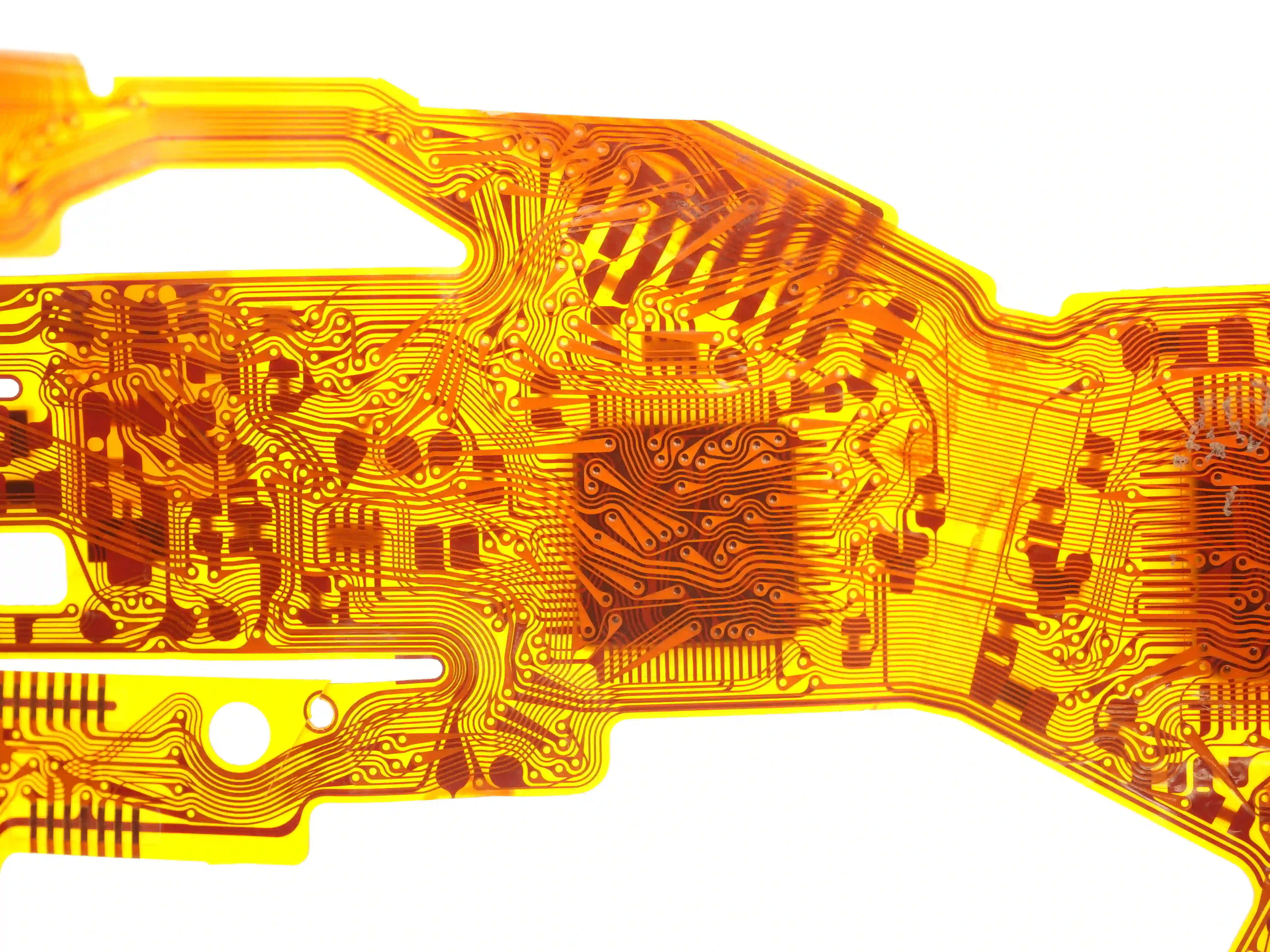
Precision Cutting for Complex 3D Flex Geometries
Rigid board routing tools apply excessive force and heat that can tear or distort thin flexible laminates. Flexible circuits therefore rely on laser cutting or precision steel-rule die cutting. Laser processes excel at intricate outlines, small retention features, and controlled bend-line scoring while introducing almost no residual stress. Die cutting is preferred for high-volume, simpler shapes because of lower cost per part.
The choice is driven by material thickness, copper weight, required edge quality, and annual volume. Designs that must fold into three-dimensional product cavities often combine both methods: laser for fine features and die for outer contour. Residual stress left by improper cutting is a frequent cause of copper cracking after thermal cycling or repeated flex. Production panels are therefore inspected for edge quality and dimensional accuracy before coverlay or stiffener operations continue.
Application-Driven Customization in Flexible Circuit Production
A smartphone display flex prioritizes ultra-thin polyimide, controlled impedance, and optional EMI shielding film. A wearable device may add pressure-sensitive adhesive for assembly and specify higher dynamic flex life. An LED strip focuses on thermal paths and continuous length. Optional processes—shielding films, selective tapes, metal reinforcement, thermal interface layers—appear only when the product physics demand them.
This level of customization means flexible PCB manufacturing cannot follow a single standardized flow. Each design is an engineered response to bend life, packaging volume, signal integrity, and environmental exposure. Early DFM reviews that define these constraints reduce both cost and schedule risk.
Table 1: Rigid vs Flexible PCB Manufacturing Focus
| Aspect | Rigid PCB (FR4) | Flexible PCB (Polyimide) |
|---|---|---|
| Base Material | Glass-reinforced epoxy | Thin polyimide film |
| Protective Layer | Liquid or dry-film solder mask | Coverlay (polyimide + adhesive) |
| Mechanical Reinforcement | Not required | Selective stiffeners (PI, FR4, stainless steel) |
| Outline Method | Mechanical routing / scoring | Laser cutting or precision die cutting |
| Primary Engineering Goal | Dimensional stability & thermal reliability | Dynamic bend life + selective rigidity |
| Typical Customization | Layer count, copper weight, surface finish | Material thickness, stiffener locations, shielding |
Table 2: Stiffener Material Selection Guide
| Stiffener Material | Typical Thickness | Best Use Case | Key Limitation |
|---|---|---|---|
| Polyimide | 0.05–0.25 mm | Ultra-thin dynamic areas, light support | Limited stiffness for connectors |
| FR4 | 0.2–1.6 mm | SMT component zones, moderate force | Higher CTE mismatch if too thick |
| Stainless Steel | 0.1–0.3 mm | High-force connectors, battery contacts | Cost and weight; requires precise bonding |
FAQ
Q1: When should coverlay be used instead of solder mask on a flexible circuit?
A1: Coverlay is required on any zone that will experience repeated dynamic flexing. Solder mask cracks and delaminates under cyclic bending; coverlay is laminated polyimide that moves with the copper and maintains dielectric protection for the required bend life.
Q2: How do stiffener locations affect flex life and assembly yield?
A2: Stiffener edges placed too close to a dynamic bend zone create stress concentrations that accelerate copper fatigue. Keep a minimum clearance (typically ≥1.5× material thickness) and verify insertion force and reflow compatibility during DFM.
Q3: What cutting method is preferred for high-volume vs complex-geometry FPCBs?
A3: Precision die cutting is cost-effective for high-volume, relatively simple outlines. Laser cutting is preferred for intricate geometries, small features, controlled bend lines, and low residual stress—especially on thinner materials.
Q4: Can the same FPCB design serve both prototype and mass production?
A4: Only if the design already incorporates the final coverlay openings, stiffener stack-up, and outline method. Changing these after prototype validation usually requires a new tooling and reliability qualification cycle.
Q5: What is the most common DFM error that shortens FPCB bend life?
A5: Leaving copper unprotected at the edge of a coverlay opening or placing a stiffener boundary inside the intended bend radius. Both create localized stress risers that initiate cracks after a few thousand cycles.
Why can this circuit board bend thousands of times… while a normal PCB shatters?
Look inside almost every modern smartphone, wearable, or folding device and you'll find them: ultra-thin Flexible Printed Circuit Boards.
They snake through impossibly tight spaces, survive constant motion, and still carry high-speed signals.
But how are these circuits actually made? And why does their manufacturing look so different from the rigid boards we already know?
The answer is not "more steps." It's a series of deliberate engineering solutions to one core problem: how do you keep copper traces electrically perfect while the entire board must remain mechanically alive?Let's go inside the factory.
Flexible PCB manufacturing actually begins on familiar ground.
It starts with a copper-clad laminate, much like a standard PCB — except the rigid FR4 core is replaced by a thin, flexible polyimide film.
From there, it follows a standard electrical playbook: holes are drilled, copper is deposited, and precise circuit patterns are etched into place.
Electrically, the foundation is identical. The conductive pathways are born the exact same way.
But mechanically... that's where everything changes.
1. Protecting the flexible circuit
Take the first hurdle: protecting copper traces that are born to move.
Conventional solder mask protects static boards well, but repeated flexing eventually creates cracks and delamination.
The solution is coverlay—a polyimide film coated with adhesive. Before being permanently laminated, precise openings are created wherever solder pads, connector contacts, or test points need to remain exposed. The coverlay is then carefully aligned, temporarily secured in position, and finally laminated under heat and pressure, forming a flexible protective layer that bends together with the copper traces.
2. Adding mechanical support exactly where it is needed
Yet, flexibility isn't always a virtue. In fact, pure flexibility can be a liability
A connector must be inserted without crushing. A chip must be soldered without the pad lifting. A battery contact needs consistent pressure.
So manufacturers selectively bond stiffeners — polyimide, FR4, or stainless steel — only in the zones that require rigidity.
The rest of the board stays fully flexible.
This hybrid behavior is impossible with a standard rigid PCB. Stiffener bonding exists to give mechanical strength precisely where physics demands it, without sacrificing the bendable regions.
3. Creating complex mechanical structures
Then comes the spatial puzzle: these circuits don't just sit flat—they must conform to complex, three-dimensional spaces.
Mechanical routing that works on thick rigid boards can tear or distort thin flexible laminates. Complex outlines, dynamic bend zones, and tiny retention features demand far higher precision.
Laser cutting and precision die-cutting are selected according to the required geometry, material, and production volume.They create clean edges, exact bend-lines, and intricate geometries while keeping residual stress minimal.
Here is what most people never realize:
Rigid PCB manufacturing is relatively standardized.
Flexible PCB manufacturing is radically customized.
A smartphone display flex may need ultra-thin materials, controlled impedance, and EMI shielding film.A wearable may add pressure-sensitive adhesive for assembly, while an LED light strip focuses on thermal paths and length.
Optional processes — shielding films, selective tapes, metal reinforcement, thermal interface layers — appear only when the product physics require them.
Each board is an engineered response to a unique combination of bend life, space, signal integrity, and environment.
Flexible PCB manufacturing shares its electrical foundation with rigid boards.
But every distinctive process exists to solve a mechanical or reliability problem that rigid manufacturing never faces.
The philosophy is constant balance:
flexibility against strength,
thinness against durability,
electrical precision against dynamic motion.
That is what makes Flexible PCB manufacturing fundamentally different.





