 00:52
00:52
Rigid PCB Design
Rigid PCB design forms the backbone of modern electronics, providing a stable and durable foundation for circuits in everything from consumer gadgets to industrial machinery. Unlike flexible alternatives, rigid printed circuit boards (PCBs) are constructed from non-bendable materials like fiberglass-reinforced epoxy, ensuring mechanical strength and reliable performance under various environmental stresses. This tag, Rigid PCB Design, encompasses a collection of articles that delve into the fundamentals, advanced techniques, and real-world applications of creating these essential components. For engineers, hobbyists, and manufacturers searching for guidance on rigid PCB design, the content here addresses key challenges such as layer stacking, trace routing, and thermal management. You'll find practical advice on selecting appropriate substrates, optimizing signal integrity to minimize noise, and incorporating design for manufacturability (DFM) principles to reduce production costs and errors. Best practices include adhering to IPC standards for via placement and solder mask application, which help prevent common issues like short circuits or component failures. These insights are particularly valuable for projects requiring high-density interconnects or compliance with regulatory requirements in sectors like automotive and aerospace. By exploring the articles under this tag, you can gain actionable strategies for prototyping and scaling designs, from initial schematic capture using tools like Eagle or Altium to final assembly considerations. Whether you're troubleshooting impedance control in high-speed circuits or integrating power distribution networks, the resources provide step-by-step approaches grounded in industry expertise. This knowledge empowers you to create more efficient, cost-effective PCBs that meet performance demands and accelerate time-to-market. Dive into specific topics to refine your skills and apply proven methods to your next electronics project.
Video Guide
-
00:52
Technical Articles
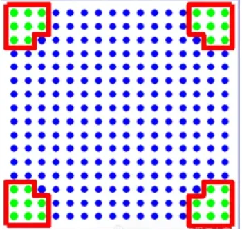
Key PCB Pad Design Guidelines for BGA SMD Components
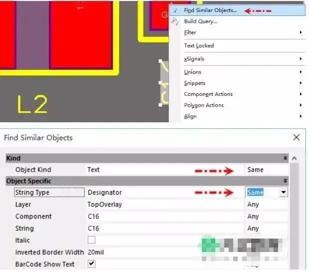
Global Editing Techniques in Altium Designer (Find Similar Objects)

Precise Spacing Control: How to Move a Diagonal Feature by Exactly 1 mm
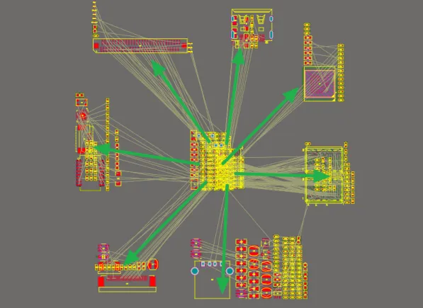
Standard PCB Design Workflow for Engineers

Crystal Oscillator Design Mistakes That Cause Intermittent Startup Failure
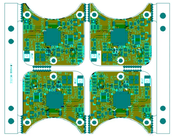
Why Adding Process Edges to a PCB Panel Is Not Wasted Board Material
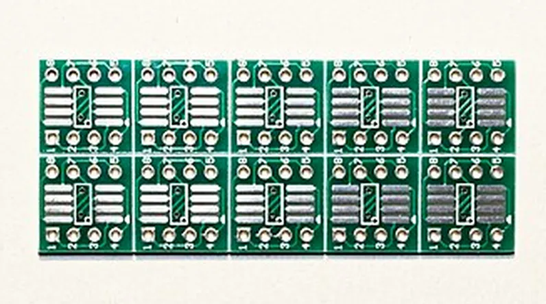
Why Do Copper Traces Near V-CUT Edges Crack During Depaneling?
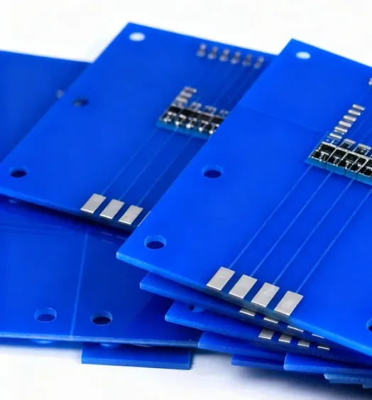
Mechanical Mounting with Non-Plated Through-Holes: Best Practices for PCBs
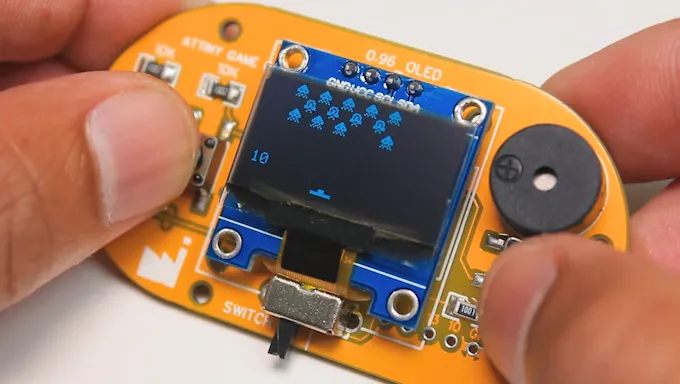
From Concept to Console: A Detailed Guide to Gaming PCB Layout

Fortifying Transactions: PCB Design for Tamper-Resistant Point-of-Sale Systems
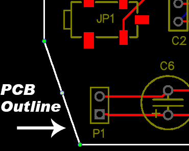
PCB Outline Essentials: Defining Board Shape, Size, and Boundaries
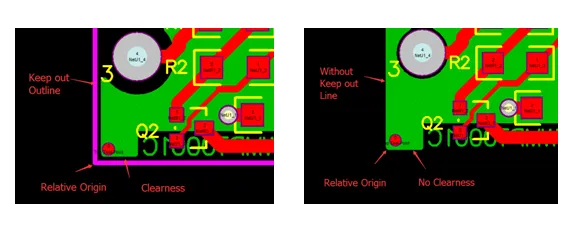
Mastering PCB Outlines: A Comprehensive Guide for Electrical Engineers

Designing Robotics Control PCBs for ROS (Robot Operating System) Integration
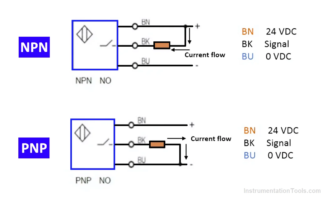
3-Wire PNP vs NPN Sensors: Wiring, PLC Integration, and Best Practices
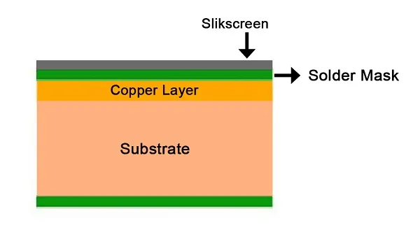
Designing for Manufacturability: Single Sided PCB Best Practices
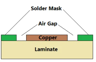
Rigid PCB Solder Mask: Protecting Your Board and Improving Solderability
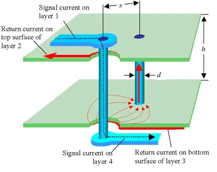
Rigid PCB Via Design Guidelines: Minimizing Inductance and Maximizing Signal Integrity
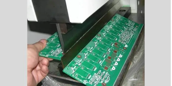
The Ultimate Guide to PCB Breakaway Rails: Enhancing Stability and Streamlining Assembly
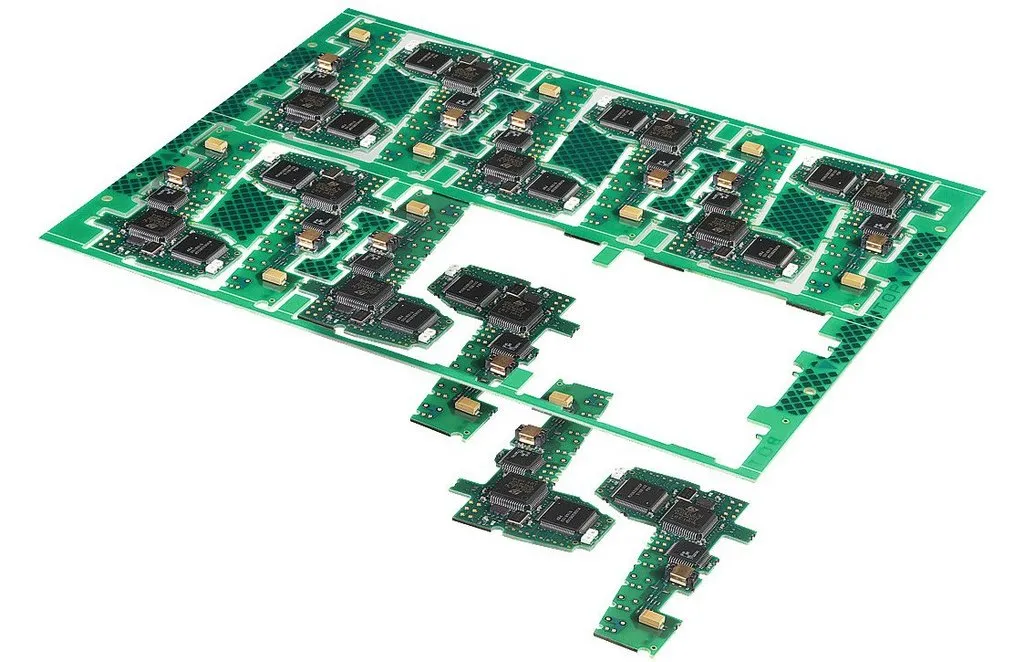
Mastering Irregular Shapes: Tab Routing for Complex PCB Panel Designs