










A clear design approach is more important than working harder. Following a standardized PCB design workflow helps avoid early mistakes that lead to major rework later. The workflow below outlines a sequence of steps to follow when designing complex PCBs.
1. Preparation of Materials
Before starting design, ensure the following materials are ready. Adequate preparation reduces design errors and avoids repeated iterations that extend the schedule.
- Schematic: Final project schematic, with all pages included in the project.
- Footprint library: PCB footprint library or component datasheets for creating new footprints.
- Mechanical drawings: DXF files that include connector positions and height restrictions.
- Design notes: Key signal handling, special chip requirements, and PCB fabrication process notes.
- Critical component datasheets: Reference layouts and routing recommendations for important parts.
2. Import Netlist
Import schematic net connections and component footprints into the PCB tool. Verify the import for discrepancies. If the schematic is updated, re-import the latest version into the PCB.
3. Import Mechanical Structure
Import board outline, component location constraints and other mechanical information into the PCB editor. If the mechanical DXF is updated, re-import it and reconcile differences immediately.
4. Project Analysis
Analyze the design at a system level before layout:
- Block diagram: Identify the main functions, modules and interfaces, and research module-specific design requirements.
- Design notes review: Interpret critical signal requirements, special chip constraints, and fabrication notes for integration into the PCB design.
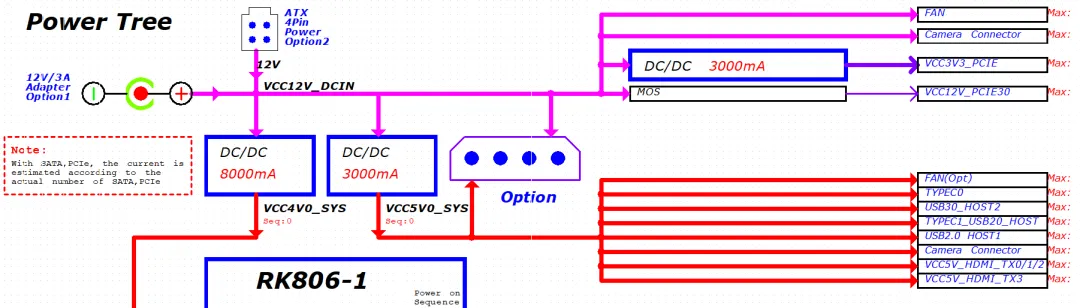
- Power tree: Analyze the project's power distribution, current requirements and flow. This is typically available in the schematic.
5. Capture Functional Modules
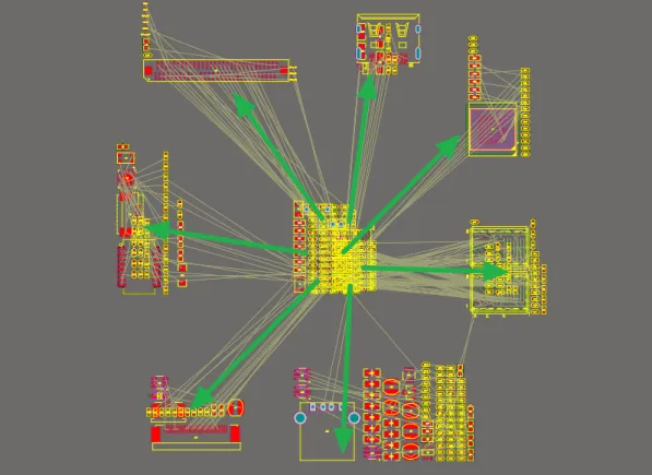
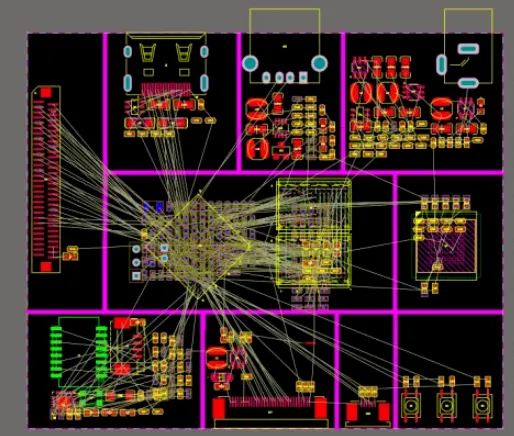
Modern products are highly integrated and often organized into functional modules. Capture components by schematic module pages so you can trace signal flow between modules and draw module guide lines on the PCB to estimate approximate placement and area.
6. Mechanical Component Placement
Using the DXF mechanical file, import the board outline and place components with fixed position requirements in their correct locations. Update placement promptly if the mechanical design changes to avoid duplicated work.
7. Key Component Placement
Place major ICs according to signal flow. This preliminary placement helps balance routing density and plan signal paths, improving the overall layout rationality.
8. Module-by-Module Placement
Complete detailed placement for each captured module, then position the modules on the PCB. This detailed placement follows the preliminary placement strategy. Observe hole and routing constraints during placement.
9. Placement Optimization
Make fine adjustments to placed components to improve layout balance and readability.
10. Stackup Configuration
Estimate the number of PCB layers required from the unrouted connections. Based on layer count and board thickness, use recommended 4-6-8 stack-ups to determine trace widths and spacing.
11. Design Rule Setup
Set trace width and spacing rules in the PCB tool to guide routing. Verify these rules against design requirements and the board fabricator's process capabilities to avoid full rework.
12. Class and Constraint Grouping
Group signals with special requirements according to IC specifications into different classes and assign corresponding routing constraints to each class.
13. Routing
Route nets so that all signals in the same network are connected. After routing, verify routing against design requirements. Check power routing for current capacity and compliance with applicable certifications.
14. Length Matching
Perform length tuning for timing-critical nets. Observe the allowable skew and length error tolerances when matching routes.
15. Routing Optimization
Improve routed traces for aesthetics and functional performance. Review and prioritize optimization for critical signals and apply best practices.
16. Power Handling
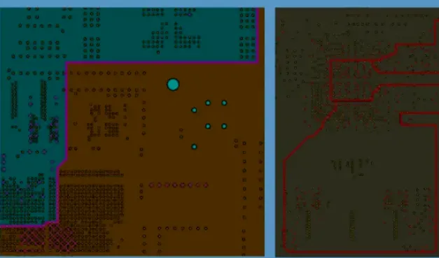
Optimize power traces and divide power planes as required. Confirm the design meets current-carrying requirements. When splitting planes, avoid routing important signals across plane boundaries.
17. DRC Checks
Run design rule checks:
- Connectivity: Verify all nets are connected and there are no open circuits.
- Other checks: Verify no shorts, avoid restricted keep-out areas, and respect component height constraints.
18. Silkscreen
Place component reference designators and add versioning and production markings (for example, ESD warnings, serial numbers, factory identifiers) in the silkscreen. Arrange silkscreen text for readability and manufacturability.
19. Project Review
Confirm all customer design requirements are met and verify manufacturing feasibility.
20. Gerber Output
Generate Gerber files from the EDA tool. For similar product families, create output templates to allow one-click Gerber generation for future revisions.
21. Gerber Verification
Even if the EDA tool has performed DRC, the generated Gerber files should be checked with industry manufacturing tools to identify producibility issues early. Use a DFM review process to catch production issues at the design stage.
22. File Archiving
Proper file archives improve communication and handoff across teams. A recommended folder structure is:
- ASM: Assembly files and top/bottom assembly drawings for the contract manufacturer.
- CAM: Gerber files, IPC netlist, and PCB manufacturing notes for the board fabricator or assembler.
- DXF: Mechanical drawing files used by the project, for the mechanical engineer.
- PCB: Final PCB project files for engineering revisions.
- SCH: Final schematic files for engineering revisions.
- SMT: Pick-and-place coordinates and stencil files for the assembly house.






