Ball grid array (BGA) packages are ubiquitous in high-density SMT assemblies and are often used for CPUs, FPGAs, and other core devices. Their fine pitch and array of solder balls deliver excellent I/O density and performance, but they also concentrate risk: suboptimal pad sizing or an inappropriate solder mask strategy can lead to opens, shorts, head-in-pillow defects, weak joints, or even device scrap. This guide focuses on BGA pad geometry and solder mask definition for lead-free (LF) reflow and consolidates practical layout rules that improve soldering yield and long-term reliability.
General Design Principles for BGA Pad Sizes
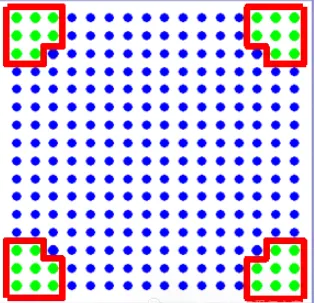
For BGAs with pitch ≥ 0.8 mm, mechanical stress during reflow and thermal cycling is often greater at the periphery, particularly at the corners. To improve joint robustness and distribute stress more evenly, use the following corner-reinforcement rule:
Corner-reinforcement rule: For each of the four corners, enlarge the nine corner pads by +2 mil relative to the standard pad size used for the interior balls.
The slightly larger landing area at the corners enhances mechanical strength and reduces the likelihood of corner-joint failures without materially affecting escape routing.

BGA Pad Size Reference Table (General Design)
| Pitch (mm) | Nine corner pads (+2 mil) | Other pads (standard) |
|---|---|---|
| 1.27 | SR27 | SR25 |
| 1.2 | SR27 | SR25 |
| 1.092 | SR22 | SR20 |
| 1.0 | SR20 | SR18 |
| 0.8 | SR16 | SR14 |
Note: SR denotes the solder mask opening (solder resist opening) diameter; the number is in mil.
SMD vs NSMD: Choosing a Solder Mask Strategy
Solder mask definition at BGA pads has a direct impact on assembly yield and joint reliability. Two strategies are widely used: SMD (solder mask defined) and NSMD (non-solder mask defined).
1. Definitions and size mapping
| Design type | Finish pad (final pad) | Copper pad (underlying copper) | Typical use |
|---|---|---|---|
| SMD (mask-defined) | A (vendor recommendation) | A + 4 mil | Specific device requirement or customer preference |
| NSMD (non-mask-defined) | A (vendor recommendation) | A (same as finish pad) | Higher wetting area and strong solder joint formation; use when copper-peel risk is controlled |
-
SMD: The solder mask overlaps the pad edge, so the finished pad is defined by the mask opening and is smaller than the underlying copper. The larger copper diameter (relative to the finish pad) improves copper adhesion to the laminate and can help with heat spreading.
-
NSMD: The solder mask does not cover the pad edge, so the pad is defined by the copper. This increases the wettable perimeter and generally promotes better solder wetting. However, because the solder fillet wraps the copper edge, there is a greater tendency for copper peel if the adhesion is weak or the board sees mechanical stress.
Both approaches are used successfully in production. SMD often helps when pad adhesion and mask registration are priorities or when the component vendor recommends it for a specific device. NSMD is commonly preferred for its wetting behavior and fillet formation, provided the PCB stackup, copper adhesion, and rework process are robust.
2. Recommended choice by pitch
The table below consolidates the corner-reinforcement rule with common solder mask strategies and can be used as a quick reference during layout. In the SMD entries, the notation SRxx–SMxx can be read as "SRxx solder mask opening; SMxx mask-defined finish pad diameter" (values in mil). For NSMD, the single SR value denotes the solder mask opening, which is equal to the copper pad diameter.
| Pitch (mm) | SMD design (mask-defined) | NSMD design (non-mask-defined) |
|---|---|---|
| 1.27 | SR29–SM25 (corner SR29) | SR25 |
| 1.2 | SR29–SM25 (corner SR29) | SR25 |
| 1.092 | SR24–SM20 (corner SR24) | SR20 |
| 1.0 | SR22–SM18 (corner SR22) | SR18 |
| 0.8 | SR18–SM14 (corner SR18) | SR14 |
Example: At 1.27 mm pitch with an SMD strategy, use a 29 mil solder mask opening at the nine corner pads and a 25 mil mask-defined finish pad. With NSMD at the same pitch, use a uniform 25 mil pad.
Connectivity and Keep-Out Rules in the BGA Region
The escape pattern, via strategy, and mechanical keep-outs beneath the device are as important as the pad itself. The following practices help reduce impedance discontinuities and improve manufacturability.
1. Connections within the "red zone" under the BGA
-
Pad to signal trace: Route out from the pad centerline rather than abruptly from a pad corner. Centerline breakout minimizes the local impedance discontinuity and helps maintain consistent trace geometry right at the pad interface.
-
Pad to via: For fine-pitch BGAs, via-in-pad plated over (VIPPO) with filled and capped vias is often required to achieve dense escapes and improve stubs and impedance control. Where manufacturing or cost constraints preclude VIPPO, a dog-bone fanout is commonly used to move vias slightly away from the pad while maintaining tight escape geometry.

Choosing between VIPPO and dog-bone involves trade-offs in assembly cost, solder voiding risk, routing density, and high-speed performance. VIPPO shortens the current path and reduces via stubs but requires a capable PCB process (via fill, cap, and flatness control) to avoid solder wicking and voids under the ball.
2. Strict keep-out constraints
Two mechanical keep-out rules help facilitate rework and reduce stress concentration under the device:
- Perimeter keep-out: Reserve a continuous 2.0 mm wide keep-out band around the outside of the BGA's outline (including CPU sockets). Avoid placing components or mechanical features in this band.
- Under-device component limit: Do not place components larger than size 3216 (1206) directly under the BGA, whether on the bottom side or on internal cavity areas.
These restrictions reduce the risk of collateral heat damage during hot-air rework and lower the chance that bulky parts will introduce local board warpage or stress that compromises BGA joints.
Summary
- Corner reinforcement: For BGAs with pitch ≥ 0.8 mm, enlarge the nine pads at each corner by +2 mil to enhance joint robustness.
- Solder mask strategy: SMD increases copper adhesion and defines the finish pad via the mask; NSMD provides larger wetting area and fillet formation. Choose per the device datasheet and process capability.
- Mechanical keep-outs: Maintain a 2.0 mm perimeter keep-out and avoid placing large parts under the BGA to enable rework and prevent stress-induced defects.
Applying these pad geometries, mask definitions, and keep-out rules yields more consistent solder joints under lead-free reflow and simplifies escape routing and rework. Use the tables above as a quick checklist when creating or reviewing BGA footprints and layouts.