










ESP32 Fingerprint Voting Machine Video: Custom 2-Layer PCB Delivers Reliable Biometrics
Key Moment
- 0:00 Introduction & Project Overview
- 1:33 AIVON PCB Sponsorship
- 1:59 Components Required
- 2:32 R503 Fingerprint Sensor Explained
- 3:15 Schematic Design
- 3:50 PCB Layout & 3D View
- 4:14 Ordering the Custom PCB
- 4:39 Assembling the Hardware
- 5:15 Coding & Libraries
- 6:23 Uploading the Code
- 6:55 System Initialization & Scan Mode
- 7:17 Web Dashboard Overview
- 8:02 Voter Enrollment Process
- 9:05 Casting a Vote & Duplicate Protection
- 9:42 Live Results, Voter Management & CSV Export
- 10:14 Outro
Project Background
Many electronics projects begin with a practical need rather than a pure experiment. In this case the goal was clear: create a fully self-contained biometric voting system that could enroll voters by fingerprint, block double-voting, accept a candidate choice through simple button presses, and stream live results to any browser—without depending on an external cloud server or paid hosting. The finished experience had to feel professional: clear OLED status messages, a clean web dashboard, and one-click CSV export of the complete voting history.
Breadboards and jumper wires are excellent for proving concepts. They are rarely adequate when an optical fingerprint sensor such as the R503 must capture clean images while an ESP32 simultaneously runs Wi-Fi, serves web pages, and maintains a stable 3.3 V rail. Contact resistance, long inductive traces, and uncontrolled ground returns quickly degrade image quality and trigger brown-outs. The moment a purpose-designed double-sided FR4 PCB arrived, the project stopped looking like a laboratory prototype and began to behave like a finished device that could be shown to real users.
This class of biometric edge system is increasingly relevant for classrooms, makerspaces, small offices, and pilot elections where data privacy, offline operation, and low cost matter. The combination of ESP32 processing power, local web server capability, and a high-performance optical sensor creates a compelling platform—provided the hardware foundation is solid.
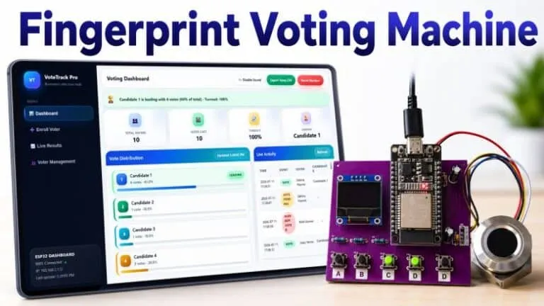
What This Video Covers
In the accompanying video, the complete development journey is demonstrated step by step. Viewers see the initial breadboard validation, the schematic drawn in EasyEDA, the transition to a clean two-layer layout, the ordering process with AIVON PCB, the arrival and assembly of the finished boards, and the final system operating reliably end-to-end.
Key sequences include voter enrollment through the self-hosted web interface (name, ID, date of birth, sex, city plus two fingerprint captures), real-time fingerprint matching that prevents re-voting, candidate selection via four active-low push buttons, live dashboard updates showing turnout and leading candidate, activity feed, full history, and CSV export. The video also highlights the mechanical and electrical improvements that only a properly manufactured PCB can deliver—short UART and I2C runs, local decoupling exactly where the R503 needs it, continuous ground pours, and solid mechanical mounting for the sensor and OLED.
Project Highlights and Key Features
- Self-contained architecture: ESP32 joins the local Wi-Fi network, serves its own web pages, and displays the IP address directly on the 0.96-inch OLED—no external server required.
- Biometric core: R503 optical sensor (up to 200 templates, UART interface, strong FAR/FRR performance) provides fast and reliable fingerprint capture and matching.
- Professional user experience: clear OLED status messages, clean multi-page web dashboard (main overview, enrollment, live results, management), and one-click CSV export of complete voting logs.
- Practical hardware choices: mostly through-hole components for easy hand assembly, female headers on ESP32, OLED and R503 for future module swaps, dedicated 6-pin terminal replacing long jumper wires, and carefully placed 10 µF electrolytic plus 0.1 µF ceramic capacitors at every critical module.
- Robust two-layer PCB parameters: FR-4, 1.6 mm thickness, 1 oz copper on both sides, lead-free HASL finish, continuous ground pours, short power and signal paths, and selective via treatment.
- Serviceability focus: critical modules kept on the top side, mechanical stability for the sensor and display, and layout decisions that prioritize noise control and reliability over extreme density.
Challenges Encountered During Development
Even a modest two-layer board reveals its weaknesses the first time the fingerprint sensor acquires an image or the Wi-Fi radio becomes active. Three interrelated issues dominated early testing.
Power integrity appeared first. The R503 draws a short, sharp current spike while capturing a fingerprint image. On a breadboard that spike frequently pulled the ESP32 into brown-out or scrambled the UART link. The sensor datasheet is explicit: supply ripple must remain under roughly 50 mV peak-to-peak or image quality collapses. Long thin power traces and inadequate local energy storage made the problem worse.
Mechanical reliability came next. Long jumper wires to the R503 connector created intermittent contacts every time a finger pressed the sensor. Flex and unreliable connections translated directly into failed captures and frustrated users.
Via treatment and copper-to-edge clearances required the same careful attention that appears in many production two-layer jobs. Design files originally showed double-sided open windows on vias while process notes called for tented vias. Left unresolved, that mismatch allows solder-mask ink to flow into the holes, leaves copper exposed at the hole mouths, and traps solder beads during HASL—defects that often pass initial electrical test yet fail later under thermal cycling. In parallel, copper-to-edge clearances that were too tight risked burrs, plating voids, and weak annular rings after depanelization.
None of these issues were exotic. They were ordinary DFM realities that separate a working demonstration from a board that can be relied upon day after day.
How AIVON PCB Helps
The creator uploaded the Gerber files, selected standard parameters, and the boards arrived from AIVON in three days. They looked clean, the holes were accurate, the solder mask was consistent, and the surface finish was ready for hand assembly. That physical quality proved decisive.
AIVON's rapid PCB manufacturing delivered short, controlled traces for the UART and I2C links, local energy reservoirs exactly where the R503 needed them, continuous ground returns for the capture current spikes, and solid mechanical mounting so the sensor and display stayed firmly in place. Female headers allowed any module to be swapped without lifting a soldering iron. The finished unit boots cleanly, displays its IP address without hesitation, accepts fingerprints without drop-outs, and keeps the live dashboard updating without unexplained resets.
Equally important was the engineering support. When via mask intent and outline data needed clarification, an Engineering Question received a prompt, precise answer. Early file review also caught copper-to-edge and via-pad issues that could have produced field failures. Manufacturing precision—consistent plating, accurate registration, clean lead-free HASL, and solid solder-mask coverage—did the quiet work that turned a promising breadboard into a device that feels finished.
The same pattern appears across many two-layer FR-4 projects handled by AIVON: responsive DFM analysis, fast-turn production, and boards that simply work the first time they are powered. For engineers moving biometric or sensor-heavy designs off the breadboard, that combination of speed, quality, and technical dialogue removes the usual sources of delay and unreliability.
Conclusion
The creative work—the system logic, the web dashboard, the enrollment flow, and the overall user experience—belonged entirely to the maker. The custom two-layer PCB simply cleared the path so that work could shine. Once the boards arrived from AIVON, the project stopped fighting the hardware and started looking like a product that could be demonstrated to anyone.
Anyone sitting on a similar idea that needs clean power delivery, solid sensor interfaces, and mechanical reliability does not need to stay on the breadboard longer than necessary. A well-reviewed board and a manufacturing partner who actually reads the files can move a project from "it almost works" to "this can be shown to real users."
FAQ
Q1: Why leave the breadboard for a custom PCB on an ESP32 + R503 project?
A1: Breadboards introduce contact resistance, long traces, and noise that the R503 will not tolerate. A proper board supplies short solid connections, correct local decoupling, and mechanical stability so fingerprint matching and Wi-Fi remain reliable day after day.
Q2: What stack-up is realistic for this class of biometric board?
A2: Standard 2-layer FR-4, 1.6 mm thickness, 1 oz copper with continuous ground pours is usually sufficient. Keep power and sensor traces short and place the decoupling capacitors exactly where the layout intends.
Q3: How critical is via tenting on a simple 2-layer fingerprint design?
A3: Selective tenting protects vias near noisy digital or power areas while leaving others open for probing. Document the intent clearly so the manufacturer does not have to guess—mismatches are a frequent source of later reliability issues.
Q4: What power practices stop the ESP32 from resetting during a fingerprint scan?
A4: Use both bulk and high-frequency capacitors right at the modules, keep the 3.3 V rail stiff, and avoid long thin power traces. The R503 itself specifies ripple under roughly 50 mV peak-to-peak.
Q5: What DFM checks should be run before sending Gerbers for an ESP32 biometric board?
A5: Verify copper-to-edge clearances, consistent via mask treatment, proper annular rings, local decoupling placement, and that any special features match the manufacturer's process capabilities. Early Engineering Questions save far more time than late surprises.
Hi everyone, it's me Ha from How to Electronics. Today I am going to show you how I designed an ESP32 based fingerprint biometric voting machine with a professional web dashboard.
This system can register voters, scan fingerprints, record votes, and display all results in real time. For this project, I used an ESP32 development board as the main controller, an R503 fingerprint sensor for biometric verification, and a 0.96 in OLED display to show system messages, fingerprint status, voter name, vote status, candidate selection, and registration progress.
The ESP32 connects to a Wi-Fi network and hosts a beautifully designed local web dashboard. The dashboard has multiple sections such as dashboard, enroll voter, live results, and voter management. The main dashboard shows live fingerprint activity, system status, latest events, and vote feed in a clean and professional layout. You can export the vote data as well and later view it in Excel or Google Sheets.
For now, let's find out how we can build this ESP32 fingerprint biometric voting machine. Let's get started.
The PCB used in this project is sponsored by Aivon, a global leader in PCB manufacturing and assembly. Aivon provides high quality PCBs with fast production and delivery times. For new users, there is currently a special campaign that includes free shipping and generous discounts, making PCB prototyping far more affordable. You can get a PCB at $1 and PCBA service as low as $35 only and with free shipping.
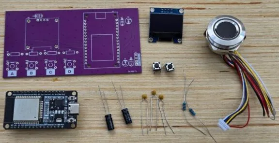
Welcome back again. Let's take a look at the components required to build this project. First, we need an ESP32 microcontroller board. Then, a fingerprint sensor. I am using an R503 capacitive fingerprint sensor, a 0.96 inch OLED display, four push buttons, some capacitors of 10 microfarads and 100 nanofarads. You can buy all of these components easily from anywhere.
Let's have a technical overview of the R503 fingerprint sensor. The R503 is an integrated biometric fingerprint module that contains an optical/capacitive sensing area, a built-in DSP processor, flash memory, and a UART communication interface. It does not send the raw fingerprint image to the ESP32 for matching. Instead, the sensor captures the fingerprint, extracts unique feature points, creates a fingerprint template, and stores this template inside its internal memory. The R503 communicates with the ESP32 using UART serial communication.
Here is the circuit diagram for this project. The ESP32 is the main controller of the system. It reads fingerprint data from the R503 fingerprint sensor through UART communication. The OLED display is connected to the ESP32 through I2C and is used to show messages. Four push buttons are connected to the ESP32 for candidate voting after fingerprint scan. Voter enrollment is done only from the web dashboard. Capacitors are added near the power supply lines to improve stability and reduce noise during operation.
After designing the schematic, I converted it into a compact PCB layout. All the components are placed on the front side for easier assembly. The routing is done based on signal requirements and component placement. Here is the 2D view of the board from the front side and also from the back side. Similarly, here is the 3D view of the board. The 3D view looks awesome.
So, the next step is to order the PCB. The Gerber files were generated and uploaded to Aivon. Uploading the Gerber file is simple. Just select the board parameters like material, thickness, solder mask, color, and quantity. And here you can see the total quote of just $1. And shipping is also free. If you want to order a PCB for just $1, click the first link in the description.
I placed the order and within a few days, I received these high quality PCBs. The finish, silk screen, and through-hole plating were excellent.
Next, I soldered all of the components for 15 minutes. The assembly was smooth, and the board looks professional once completed. For ESP32 and OLED display, I'm using a female header. I could insert all of the components easily here. For the R503 fingerprint sensor, I used wires as this sensor needed to be placed in a particular position.
Now, let's move on to the coding part. We will develop a C++ code to interface the R503 fingerprint sensor and OLED display with ESP32 and visualize the fingerprint voting on a web page.
The code starts by including the required libraries for the project. The Adafruit fingerprint library is used for R503 communication with the ESP32. The Adafruit GFX and Adafruit SSD1306 libraries are used to control the OLED display. In the Wi-Fi section, the SSID and password are added so the ESP32 can connect to the local network.
The main loop continuously checks fingerprint scans and candidate button presses. These events are displayed on the OLED screen, printed on the serial monitor, and sent to the web dashboard as JSON data through the API routes.
Here is the header file for the project. The dashboard.h file contains all the HTML, CSS, and JavaScript code used to create the live web view.
Once the hardware assembly is complete, it's time to upload the code. To upload the code, connect the type-C USB cable directly to the ESP32. In the Arduino IDE, go to tools, board, and select ESP32 dev module. Then, choose the correct COM port. Finally, click the upload button. The code will then be uploaded to the ESP32 board.
After uploading the code to the ESP32, the device starts initializing all of the connected modules. Once the ESP32 connects to the local Wi-Fi network, it displays the IP address on the OLED screen. Finally, the system enters scan mode.
To access the web dashboard, enter the IP address on a web browser. The dashboard page shows the live fingerprint system status, Wi-Fi connection, latest API update time, and live vote activity feed. From the left side menu, we can open different sections such as dashboard, enroll voter, live results, and voter management.
To register a new voter, open the ESP32 web dashboard and go to the enroll voter section. Here, enter the voter details such as name, ID number, DOB, sex, and city. Then click the start registration button.
After starting the registration, the dashboard shows an enrollment started pop-up and the OLED display asks the user to place a finger on the R503 fingerprint sensor. The sensor first captures the fingerprint image, then asks the user to remove the finger and place the same finger again for the second scan. Once both scans are matched successfully, the fingerprint template is saved in the R503 sensor memory and the voter details are stored in the ESP32. The OLED display shows a success message and the dashboard also displays a registration successful popup with the voter name, fingerprint ID, ID number, and city.
After registration, a registered voter can scan their finger, press a candidate button, and cast one vote during the election. When the voter selects a candidate, the dashboard displays a vote success popup with the voter name, fingerprint ID, ID number, and selected candidate.
If the same voter scans again after already voting, the system blocks duplicate voting and displays an already voted message on the dashboard. The dashboard also keeps updating the live vote feed, live results, and voter records.
In the live results section, vote counts and vote history are shown with name, ID number, finger ID, candidate, and message. The voter management section shows all registered voters along with their assigned fingerprint IDs and a delete option.
The dashboard also provides an export votes CSV option. This allows the vote history to be downloaded as a CSV file which can be opened in Excel or Google Sheets for record keeping.
That's all from the video part today. I hope you like this video. So why not drop a like and hit the subscribe button. Finally, thank you so much for watching. See you in the next video.





