Many maker projects begin with the same quiet spark: "Wouldn't it be useful if..." This one started with a clear goal. The creator set out to build a self-contained biometric voting system that could enroll voters by fingerprint, prevent double-voting, let people select a candidate with a simple button press, and push live results to any browser—without relying on an external server. The experience also needed to feel finished: clear OLED prompts, a professional web dashboard, and the ability to export results as CSV.

Breadboards and jumper wires can prove a concept. They rarely deliver the reliability or the clean appearance a system like this requires. The moment a custom PCB arrived, the project stopped looking like a laboratory experiment and started feeling like a finished device.
Watching the Idea Come Alive on the Bench
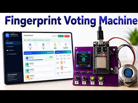
The sequence is simple and effective. A voter places a finger on the R503. The OLED responds at once with status. The ESP32 matches the stored template, confirms the fingerprint has not already voted, and opens a short voting window. Four push buttons stand ready. One press records the choice, the dashboard updates in real time, and that fingerprint is locked for the rest of the election.

Everything runs on the ESP32 itself. The board joins the local Wi-Fi network, serves its own web interface, and displays the IP address directly on the OLED. Any browser can open clean pages for the main dashboard, voter enrollment, live results, and management. Turnout, leading candidate, activity feed, full history, and CSV export are all available. Enrollment happens through the same web interface—name, ID number, date of birth, sex, city—followed by two finger scans so the R503 can store a reliable template.

The hardware choices remain practical: ESP32 as the controller, R503 optical sensor (200 templates, UART, strong FAR/FRR performance), 0.96-inch OLED, four active-low buttons with internal pull-ups, and carefully placed capacitors for clean power. The schematic was drawn in EasyEDA. Most components stayed through-hole. Critical modules sat on the top side. Female headers made later module swaps straightforward. The finished unit looks and behaves like something that could be shown to real users rather than a tangle of wires on a bench.
Figure: ESP32 Fingerprint Voting Machine Hardware
Looking Closer at the Board That Carried It
The PCB that supported the entire system is a clean double-sided design.
|
Parameter |
Typical Value Used |
|---|---|
|
Layers |
2 |
|
Material |
FR-4 |
|
Thickness |
1.6 mm (selectable at order) |
|
Copper |
1 oz both sides |
|
Finish |
Lead-free HASL |
|
Component approach |
Mostly through-hole + female headers |
|
Placement priority |
ESP32, OLED, R503 headers and buttons on top |
|
Local power support |
10 µF electrolytic + 0.1 µF ceramic near modules |
|
Signal routing |
Short UART to sensor, short I2C to OLED |
Ground pours remained continuous. Power paths stayed short. A dedicated 6-pin terminal replaced long jumper wires to the R503. The layout favored serviceability and noise control rather than packing density for its own sake.

The Moments the Hardware Pushed Back
Even a modest 2-layer board can reveal its weak points the first time the fingerprint sensor captures an image or the Wi-Fi radio wakes up.
Power integrity appeared first. The R503 draws a short, sharp current spike while acquiring the fingerprint image. On a breadboard that spike often pulled the ESP32 into brown-out or scrambled the UART link. The sensor datasheet is clear: ripple must stay under roughly 50 mV peak-to-peak or image quality suffers. Placing bulk and high-frequency capacitors directly at the modules, shortening the 3.3 V runs, and maintaining a solid ground return path eliminated the resets.
Mechanical reliability came next. Long jumper wires to the R503 connector created intermittent contacts every time a finger pressed the sensor. Moving to a proper PCB terminal plus female headers removed the flex and the unreliable connections at the same time.
Via treatment required the same care that appears in many 2-layer jobs. On a recent production run the design files showed double-sided open windows on vias while the process notes called for tented vias.

Left unresolved, that mismatch allows solder-mask ink to flow into the holes, leaves copper exposed at the hole mouths, and traps solder beads during HASL—defects that often pass initial electrical test and fail later under thermal cycling. An Engineering Question clarified the intent and the mask files were corrected. The same disciplined approach kept digital noise away from the fingerprint and display paths on this voting board.
None of these issues were exotic. They were ordinary DFM realities that separate a working demonstration from a board that can be relied upon day after day.
What Changed Once the Boards Arrived from AIVON
The creator uploaded the Gerber files, selected standard parameters, and the boards arrived in three days. They looked clean, the holes were accurate, the mask was consistent, and the surface finish was ready for hand assembly. That physical quality proved more important than it first appeared.

The custom board delivered short, controlled traces for the UART and I2C links, local energy reservoirs exactly where the R503 needed them, continuous ground returns for the capture current spikes, and solid mechanical mounting so the sensor and display stayed firmly in place. Female headers allowed a module to be swapped without lifting a soldering iron. The finished unit boots cleanly, displays its IP address without hesitation, accepts fingerprints without drop-outs, and keeps the live dashboard updating without unexplained resets.

The same pattern appears across many 2-layer FR-4 projects. On another recent panel, copper-to-edge clearances were too tight and several via pads were asymmetric. Those issues risked burrs, plating voids, and weak annular rings after depanelization. Early review caught the problems, the attributes were clarified, and the boards shipped on schedule with no later field complaints. The same careful file review and process alignment turned this voting machine from a promising breadboard into a device that feels finished.

Manufacturing precision did the quiet work: consistent plating, accurate registration, clean HASL, and solid solder-mask coverage. The headers seated properly, the buttons felt positive, and the power capacitors performed without coupling noise into the sensor. Responsive engineering support meant small questions about mask openings or outline data received quick answers, allowing the creator to keep moving instead of waiting.
In the end the board did not invent new features. It simply removed the noise, the intermittents, and the mechanical fragility that usually keep biometric prototypes stuck in the "almost ready" stage.
A Few Checks That Matter on Boards Like This
|
Check |
Why it matters on this kind of project |
Practical rule |
|---|---|---|
|
Local decoupling placement |
R503 image quality collapses with high ripple |
0.1 µF + 10 µF within 5 mm of the power pins |
|
Via mask intent |
Noise isolation versus test access |
State selective tenting clearly in the fab notes |
|
Header strategy |
Easy module swaps and field service |
Female headers on ESP32, OLED and R503 |
|
UART / I2C trace length |
Signal integrity at 3.3 V |
Keep under 50 mm wherever possible |
|
Ground continuity |
Return path for the sensor's capture current spike |
Solid pour both sides, avoid unnecessary slots |
|
Copper-to-edge clearance |
Prevent burrs and exposed copper after routing |
≥ 0.2 mm from routing edges, more for V-cut |
Looking Back from the Factory Floor
The creative work—the system logic, the web dashboard, the enrollment flow, the user experience—belonged entirely to the maker. The custom 2-layer PCB simply cleared the path so that work could shine. Once the board arrived, the project stopped fighting the hardware and started looking like a finished product.
Anyone sitting on a similar idea that needs clean power, solid sensor interfaces, and mechanical reliability does not need to stay on the breadboard longer than necessary. A well-reviewed board and a manufacturing partner who actually reads the files can move a project from "it almost works" to "this can be shown to anyone."
FAQ
Q1: Why leave the breadboard for a custom PCB on an ESP32 + R503 project?
A1: Breadboards add contact resistance, long traces and noise the R503 will not tolerate. A proper board gives short solid connections, correct local decoupling and mechanical stability so fingerprint matching and Wi-Fi stay reliable day after day.
Q2: What stack-up is realistic for this class of biometric board?
A2: Standard 2-layer FR-4, 1.6 mm, 1 oz copper with continuous ground pours is usually enough. Keep power and sensor traces short and place the decoupling capacitors exactly where the layout intends.
Q3: How critical is via tenting on a simple 2-layer fingerprint design?
A3: Selective tenting protects vias near noisy digital or power areas while leaving others open for probing. Document the intent clearly so the manufacturer does not have to guess—mismatches are a frequent source of later reliability issues.
Q4: What power practices stop the ESP32 from resetting during a scan?
A4: Use both bulk and high-frequency capacitors right at the modules, keep the 3.3 V rail stiff, and avoid long thin power traces. The R503 itself specifies ripple under roughly 50 mV peak-to-peak.
Q5: Are female headers acceptable if the board might see light production use?
A5: Yes for prototypes and small runs. They make module replacement easy and reduce the risk of damaging the PCB when a sensor or display needs swapping. Higher volume can move to direct soldering later if needed.
Q6: What DFM checks should be run before sending Gerbers for an ESP32 biometric board?
A6: Verify copper-to-edge clearances, consistent via mask treatment, proper annular rings, local decoupling placement, and that any special features match the manufacturer's process capabilities. Early Engineering Questions save far more time than late surprises.