










PCB Soldering Basics: Through-Hole and SMD Techniques Explained
What This Video Covers
This video provides essential PCB soldering fundamentals for beginners, covering the basic tools, safety practices, and step-by-step techniques for both through-hole and surface mount components.
Key topics include proper equipment setup (soldering iron, solder wire, flux), safety measures like fume extraction and temperature control (320–350°C), and correct soldering methods. For through-hole components, the process involves heating the pad and pin, feeding solder to form a smooth, shiny joint resembling a small volcano. SMD soldering follows similar principles with flux application and tacking components in place.
The video highlights critical beginner mistakes to avoid: insufficient temperature causing cold joints, excessive solder leading to bridges, and prolonged heating that damages pads or components. These skills directly improve outcomes during PCB prototype and PCB assembly projects.
Understanding proper soldering techniques helps engineers and technicians create more reliable boards for applications ranging from consumer electronics PCB to industrial control PCB, reducing defects and enhancing overall manufacturing quality.
Key Highlights
- Proper through-hole soldering requires heating both pad and pin, then feeding solder to form a shiny, volcano-shaped joint for strong electrical and mechanical connections.
- SMD soldering uses flux and a tacking method, with the same core principles as through-hole but adapted for smaller surface pads.
- Avoid common errors like cold joints, solder bridges, and overheating to ensure reliable, professional-quality PCB solder connections.
Essential Tools and Safety Practices for Reliable Soldering
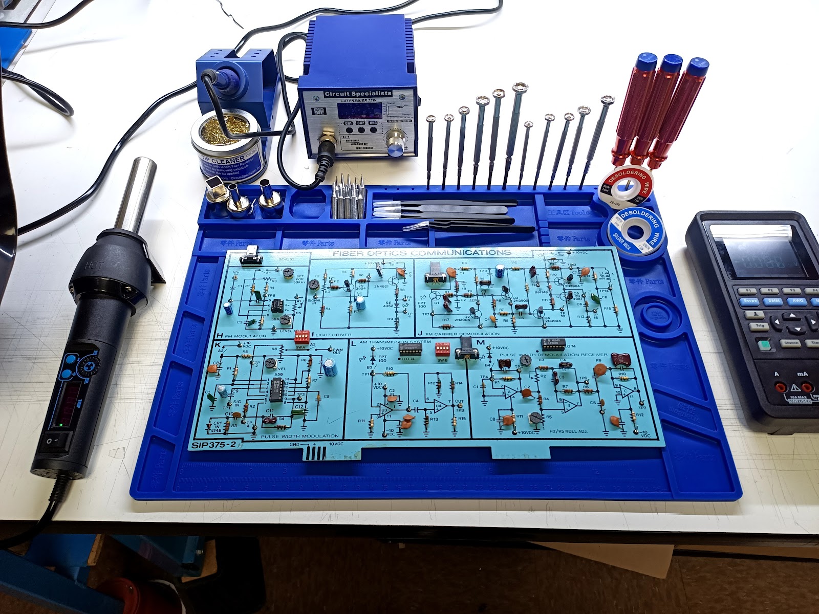
High-quality soldering begins with appropriate equipment selection. Temperature-controlled soldering stations with adjustable settings between 300–380°C provide the necessary precision for both leaded and lead-free processes. Fine-tip irons facilitate access to dense SMD pads, while chisel tips handle larger through-hole connections more effectively.
Flux is indispensable for removing oxides and promoting solder wetting. No-clean or rosin-based fluxes are common in production environments, but proper ventilation or fume extraction systems must be used to protect operators from harmful vapors. Personal protective equipment, including safety glasses and ESD-safe workstations, prevents component damage and ensures operator safety during manual assembly.
In manufacturing settings, consistent tool maintenance—such as regular tip cleaning and calibration—directly impacts joint quality. Poorly maintained equipment leads to inconsistent heat transfer and increased defect rates, particularly during prototype iterations where manual soldering is prevalent.
Step-by-Step Through-Hole and SMD Soldering Methods
Through-hole soldering begins with component insertion and lead trimming to the correct length. The iron tip heats both the pad and lead simultaneously for 2–3 seconds before applying solder wire to the opposite side, allowing capillary action to form a concave fillet. The ideal joint exhibits smooth, shiny appearance without cracks or excessive solder.
SMD soldering requires precise flux application to pads prior to component placement. Tacking one or two leads stabilizes the part, followed by sequential soldering of remaining terminals. Drag soldering techniques with a fine tip and ample flux enable efficient processing of multi-pin components such as SOIC or QFP packages while minimizing bridge formation.
Real production environments emphasize controlled timing and heat application to avoid thermal shock to sensitive components. Overheating can delaminate pads or degrade internal die attachments, while insufficient heat produces high-resistance cold joints that fail under vibration or thermal cycling.
Common Defects and Prevention Strategies in PCB Assembly
Cold joints represent one of the most frequent issues in manual soldering, resulting from inadequate heating or contaminated surfaces. These joints appear dull and grainy, leading to intermittent connections and field failures. Prevention involves proper surface preparation, correct temperature selection, and verification of solder flow before removing the iron.
Solder bridges occur when excess solder connects adjacent pads, creating shorts that are particularly problematic on fine-pitch SMD components. Using appropriate solder wire diameter (0.5–0.8 mm for SMD work) and applying flux generously helps control flow. Wick or desoldering tools allow clean removal of bridges during rework without damaging traces.
Lifted pads and component damage arise from prolonged heat exposure or aggressive mechanical force. DFM guidelines recommend adequate pad size, thermal relief connections where appropriate, and training operators on heat management. In volume production, these defects contribute significantly to scrap rates and rework costs.
Practical DFM Tips for Better Soldering Outcomes
Designers should specify pad geometries that accommodate both manual and automated processes. Through-hole pads benefit from annular ring widths of at least 0.3–0.5 mm for mechanical strength, while SMD pads require precise sizing to match component terminals and stencil apertures.
Component orientation and spacing influence soldering accessibility. Grouping similar package types and providing adequate clearance reduces operator fatigue and improves consistency. For mixed-technology boards, sequencing assembly steps—typically through-hole first followed by SMD—optimizes workflow and minimizes thermal stress on previously soldered joints.
Material selection also plays a critical role. Lead-free solder alloys require slightly higher temperatures and more active fluxes compared to traditional tin-lead compositions, affecting process windows. Early design reviews with manufacturing partners help align layout decisions with production capabilities, ultimately improving first-pass yields and long-term reliability.
Aspect Comparison
| Aspect | Through-Hole Soldering | SMD Soldering | Common Risks |
|---|---|---|---|
| Typical Temperature | 320–350°C | 300–340°C | Overheating / Cold joints |
| Key Technique | Heat pad + pin, feed solder | Flux, tack, drag or point solder | Bridges, lifted pads |
| Inspection Method | Visual | Visual + AOI | Hidden defects in dense areas |
| Rework Difficulty | Moderate | Higher for fine-pitch | Component damage |
FAQ
Q1: What temperature should you set for PCB soldering?
A1: Set your soldering iron to 320–350°C for most standard PCB work with leaded or lead-free solder to ensure proper flow without damaging components or pads.
Q2: What are the most common beginner mistakes in PCB soldering?
A2: The most frequent issues are using too low a temperature (cold joints), applying too much solder (bridges/shorts), and heating joints for too long (lifted pads or damaged components).
Q3: How do you solder SMD components on a PCB?
A3: Apply flux, tin the iron tip, tack one side of the component to hold it, then solder the remaining pads while ensuring good wetting and avoiding excess solder.
Q4: How does proper flux application impact soldering quality?
A4: Flux removes surface oxides and improves solder wetting, resulting in stronger, more reliable joints. Insufficient flux leads to poor flow and cold joints, while excess residue may require additional cleaning in sensitive applications. Selection of flux type should match the solder alloy and final product requirements.
Q5: What are the differences in soldering leaded versus lead-free solder?
A5: Lead-free alloys typically require higher temperatures and exhibit poorer wetting characteristics, narrowing the process window. This increases risks of thermal damage and incomplete joints. Manufacturers often adjust stencil designs and reflow profiles accordingly when transitioning to lead-free processes for compliance reasons.
Want to learn soldering? You only need: a soldering iron, solder wire, flux, and some old circuit boards to practice on.
First, safety.
Turn on your fume extractor, wear safety glasses, and set your iron to 320–350°C.
Start with the easiest — through-hole soldering.
Insert the component straight.
Touch the pad and the pin with the iron tip for 1–2 seconds.
Feed solder wire on the opposite side until it flows and wraps the pin.
Remove the solder, then remove the iron. Hold still for one second while it cools.
Good joints should look shiny and smooth like a small volcano.
For SMD, it's almost the same.
Add a bit of flux → tin the iron tip → tack the component, then solder the rest.
Avoid these beginner mistakes:
Too low temperature = cold joints (dull and weak)
Too much solder = bridges and shorts
Heating too long = damaged pads
Practice more and your joints will get better naturally.
Like and save this video. See you in the next one!





