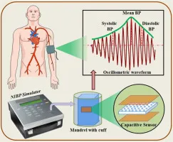
Oscillometric Bluetooth 4.0 Electronic Blood Pressure Monitor Design
Technical overview of an oscillometric Bluetooth 4.0 electronic blood pressure monitor: hardware (pump, sensor, STM32), signal conditioning, Android app, and accuracy results.
Medical Electronics represents a vital intersection of advanced technology and healthcare, where electronic systems and printed circuit boards (PCBs) power life-saving devices and diagnostic tools. This category delves into the design, development, and optimization of electronics tailored for medical applications, addressing the unique challenges of reliability, precision, and regulatory compliance in environments where accuracy can mean the difference between health and harm. From wearable health monitors that track vital signs in real time to sophisticated imaging equipment like MRI machines and pacemakers, Medical Electronics encompasses a wide array of innovations that enhance patient care and streamline clinical workflows. Professionals in this field must navigate stringent standards such as ISO 13485 and FDA guidelines, ensuring devices are safe, effective, and resistant to electromagnetic interference. The practical value lies in empowering engineers, designers, and healthcare innovators to create solutions that improve diagnostics, enable remote monitoring, and support personalized medicine, ultimately contributing to better outcomes in hospitals, clinics, and home settings. This category offers comprehensive guides on PCB layout for medical-grade components, tutorials on integrating sensors and microcontrollers into diagnostic tools, and insights into emerging trends like telemedicine and AI-driven health analytics. Best practices cover everything from thermal management in implantable devices to signal integrity in high-stakes environments. By examining these resources, readers gain actionable knowledge to tackle real-world projects, whether prototyping a new blood glucose meter or optimizing circuits for surgical robots. Staying informed on these topics equips you with the expertise to drive advancements in healthcare technology. Dive into the articles here to uncover strategies that bridge electronics engineering with medical needs, fostering innovations that transform patient experiences and operational efficiency.
Technical overview of an oscillometric Bluetooth 4.0 electronic blood pressure monitor: hardware (pump, sensor, STM32), signal conditioning, Android app, and accuracy results.
Technical overview of medical power architecture for patient-connected devices, addressing insulation, EMC, MOPP strategies and patient leakage limits.
Design of a hanging infusion monitor using a load cell and HX711 ADC to compute remaining infusion time, show progress, alarm on completion, and transmit status wirelessly.
Technical overview of a portable ECG front-end amplifier: PCB isolation, shielding, component placement, and IIR/notch digital filters for interference suppression.
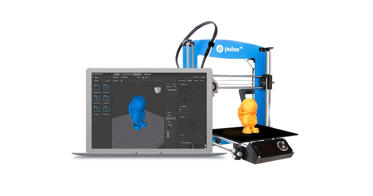
Design and implementation of an embedded framebuffer driver for an FDM 3D printing image control system to print patient-specific bone models for orthopedic surgery.
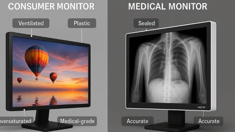
Comparison of medical vs consumer displays covering DICOM Part 14, grayscale depth, luminance, resolution, contrast, response time, safety and certification.
Discover expert PCB design and manufacturing strategies for medical electronics. Learn how to achieve superior signal integrity, EMI/EMC compliance, power efficiency, and reliability in wearable medical devices, infusion controllers, and portable diagnostic systems.
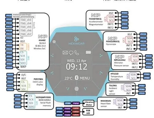
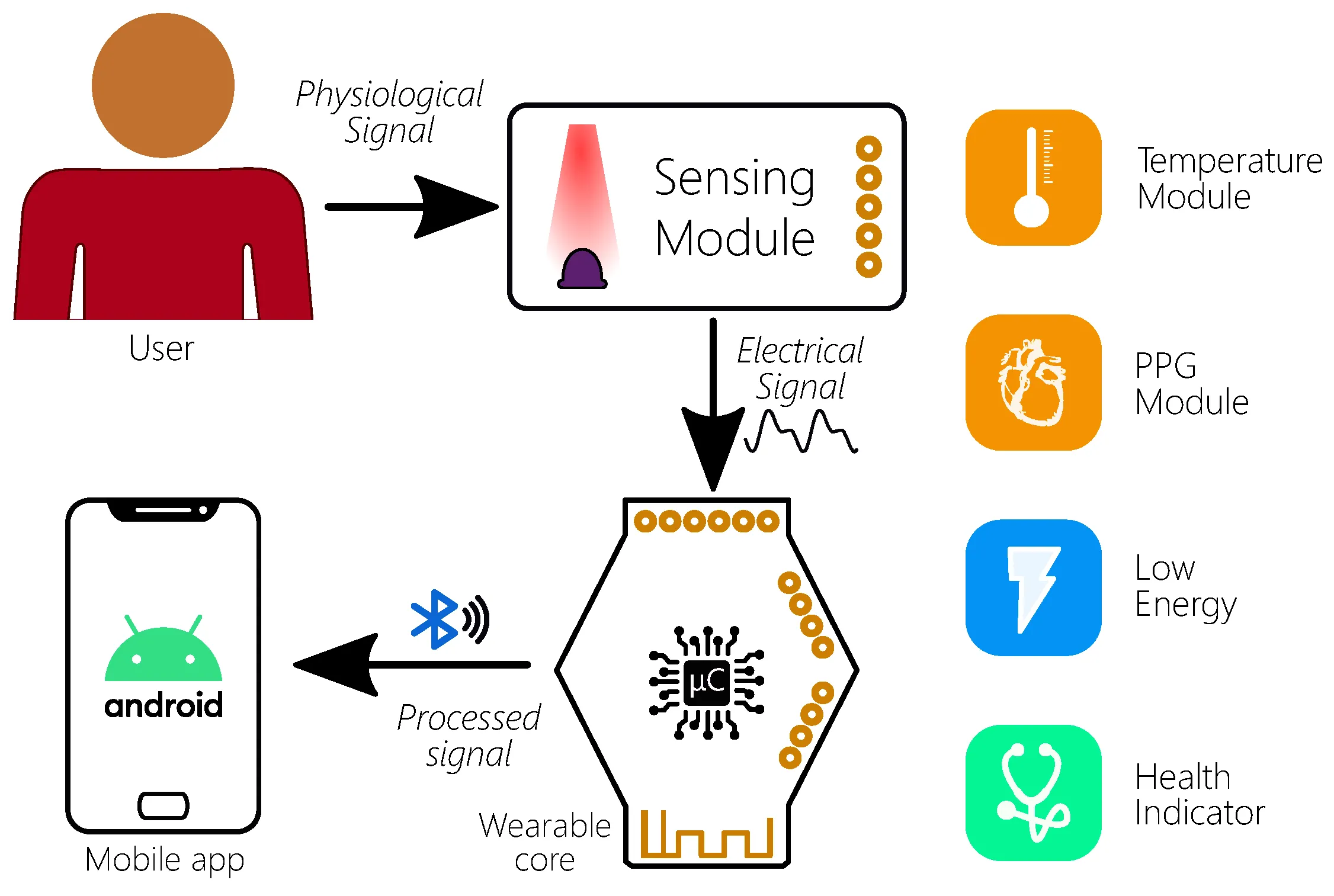
Guide to prototyping wearable medical devices with off-the-shelf Wi?Fi modules, covering module selection, RF considerations, certification, and development tradeoffs.
Technical overview of IEC 60601-1 applied-part power systems, comparing secondary DC/DC isolation and high-power BF/CF supply designs to meet patient leakage current limits.
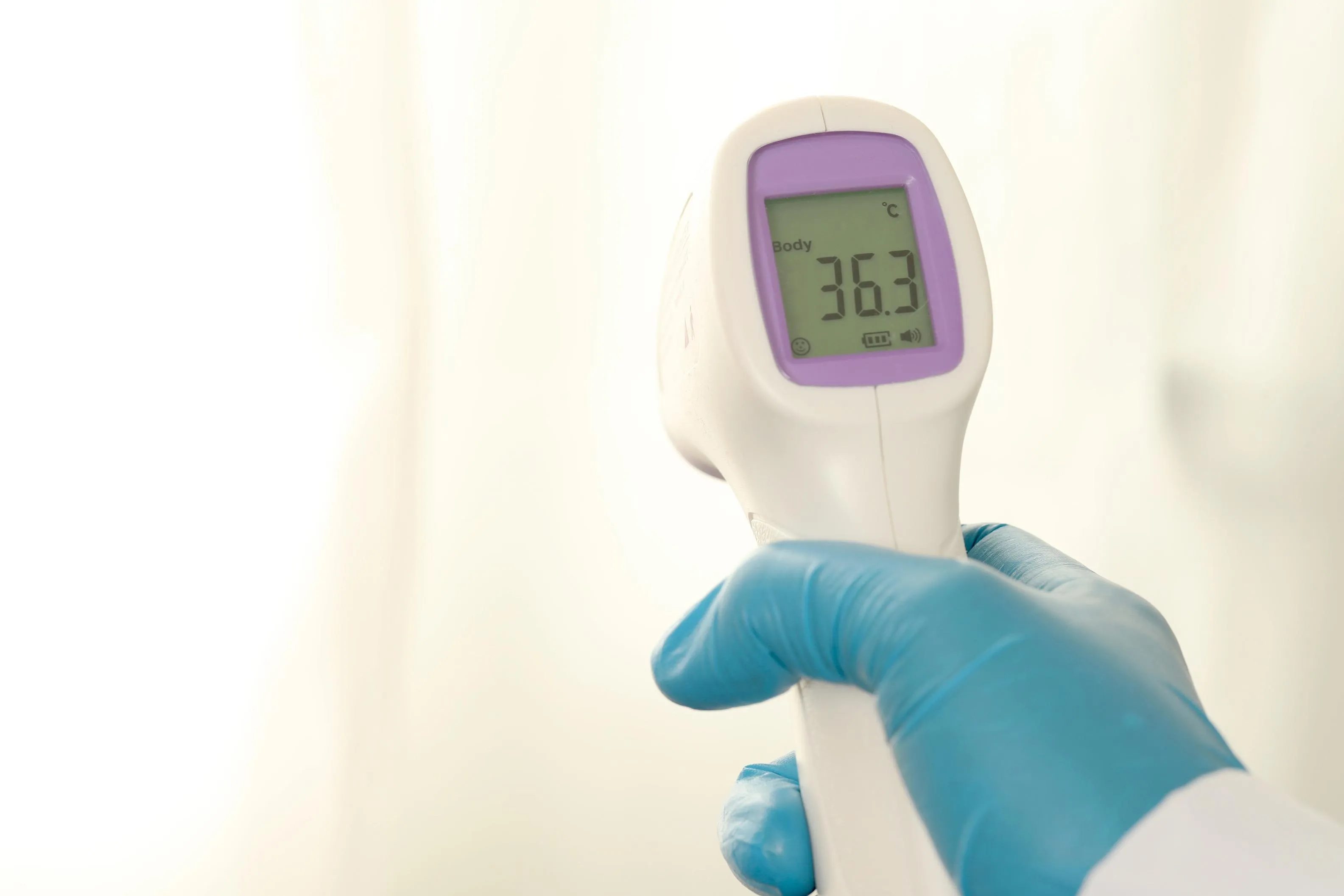
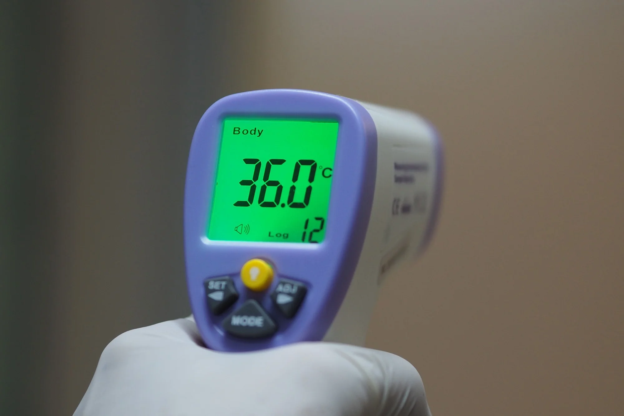
Overview of forehead thermometer design and accuracy factors, covering infrared thermopile sensors, compensation algorithms, and an SD8709 single-chip 24-bit ADC MCU solution.
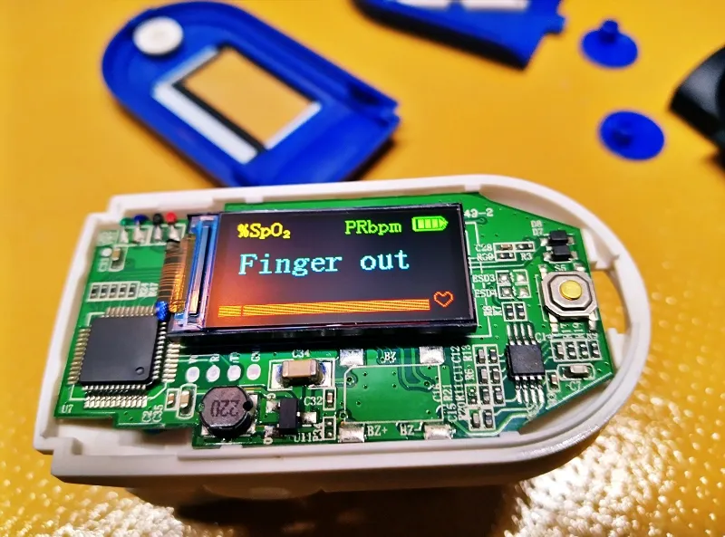
TS951X front-end analog family for finger-clip pulse oximeters: integrated I?F converter, H-bridge LED drive, low-power operation; TS9514 analog and TS9517 digital dimming.
Learn PCB design strategies for medical infrared thermometers. Discover optimized layouts, low-noise analog routing, thermal management, power efficiency, and manufacturing best practices that deliver accurate non-contact temperature measurement and long-term device reliability.