










Decode PCB Markings Part 2: Power Rails, Serial Buses, and Control Labels
What This Video Covers
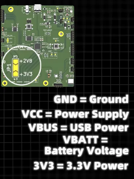
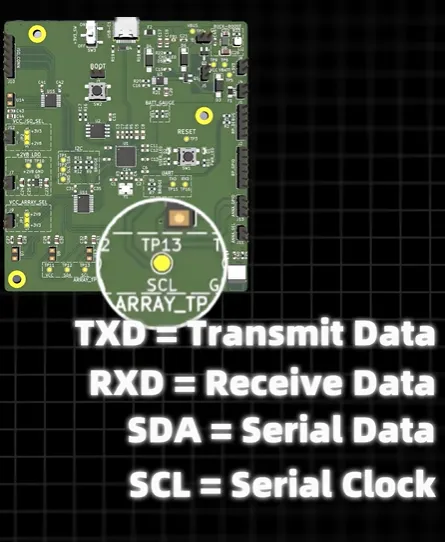
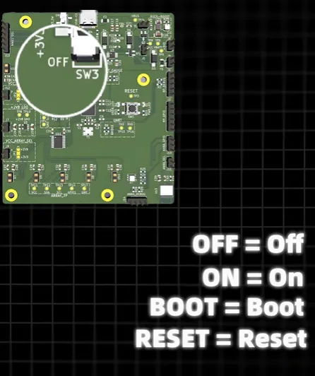
Part I of this series decoded component reference designators (R, C, U, Q). Part II is different: it reads the net and function labels printed next to connectors, headers, and pads. In 36 seconds the video maps the marks on a real production board—GND (ground), VCC (board supply), VBUS (USB power), VBATT (battery voltage), 3V3 (3.3 V rail), TXD/RXD (UART), SDA/SCL (I2C), ON/OFF, BOOT, RESET, and TP (test point).
Those strings are not part types. They tell an engineer which copper net a pin belongs to, which rail to probe first, and which pad brings a microcontroller out of reset. That is the language used on PCB prototype bring-up and on turnkey PCB assembly first-article. The same labels show up on USB-battery products, consumer electronics PCBs, and industrial control heads. Watch the short, then use the tables below when you review Gerbers or write a fixture map before requesting a PCB quote.
Key Highlights
- Power words on the legend name the rail, not the component: GND is the return, VCC is the board supply, VBUS is USB 5 V, VBATT is the battery node, and 3V3 is the regulated 3.3 V rail.
- TXD/RXD mark UART data direction; SDA/SCL mark the I2C data and clock pair—swap TXD with RXD and the port will not enumerate.
- ON, OFF, BOOT, RESET, and TP are control and access points: they tell assembly and test where the switch, boot strap, reset net, and probe pad sit.
Power Rail Labels on the Silkscreen: GND, VCC, VBUS, VBATT, and 3V3
The board in the video is a compact USB-plus-battery card. The legend therefore spends most of its ink on power geography, because that is what you probe before you talk to the MCU.
GND is the return. On mixed boards you may also see AGND, PGND, or CHASSIS; this short uses the single common mark. Probe here first when a rail looks dead—many "no 3V3" tickets are a missing return, not a dead regulator.
VCC is the board's main supply node after regulation or after the input selector. It is not a voltage number. On 3.3 V logic cards VCC often is 3.3 V; on 5 V USB accessories it may be 5 V. Read VCC as "this copper is the primary rail," then confirm the voltage on the schematic.
VBUS is specifically USB bus power—typically 5 V from the host or a Type-C controller. It is upstream of the battery charger and of the 3.3 V LDO. If VBUS is missing, the USB PHY and the charge path are both unpowered even when VBATT is healthy.
VBATT is the battery or charger output node. It can sit above or below VBUS depending on topology (charge-through vs. power-path). Do not short VBATT to VBUS on the bench; the silkscreen exists so those two islands stay distinct during bring-up.
3V3 is the regulated 3.3 V logic rail that feeds the MCU, I2C pull-ups, and most of the data section. On the video board it sits downstream of an LDO. If 3V3 is missing while VBUS or VBATT is present, the fault is the regulator, its enable, or a short on the logic island—not the USB connector.
| Label | Meaning in this video | Typical voltage / role | First probe use |
|---|---|---|---|
| GND | Ground / return | 0 V reference | Scope ground clip; continuity to connector shell if designed that way |
| VCC | Main board supply | Often 3.3 V or 5 V—confirm on the schematic | Confirm the card is powered after the input selector |
| VBUS | USB power | ~5 V from the host | Confirm the USB connector and cable path |
| VBATT | Battery voltage node | Cell / pack voltage; charger output | Separate battery path from USB path |
| 3V3 | 3.3 V logic rail | 3.3 V after the LDO | MCU, pull-ups, and I2C section |
For power supply PCB and new energy layouts the same five names scale up (12 V, 48 V, PACK+), but the rule does not change: the legend names the net, the datasheet names the voltage.
Serial and Data Marks: TXD, RXD, SDA, and SCL
After the rails, the video points at the debug and sensor buses.
TXD is transmit data from the local UART. RXD is receive data into the local UART. These marks are printed on header pins and connector pads so a USB-UART cable can be attached without opening the schematic. The manufacturing trap is crossed pairing: the board's TXD must go to the adapter's RXD. If both sides print "TXD" and you wire them together, the port stays silent. Put the label on the board pin, not on the imagined far-end device.
SDA is I2C serial data. SCL is I2C serial clock. They travel as a pair. Silkscreen that labels only one pad of a two-pin header creates first-article errors when the fixture is wired from the photograph. Keep SDA and SCL next to their own pads, at the same height, and off the landing pattern so the ink does not sit in paste.
These four marks are how a consumer electronics or IoT bring-up board gets a console and a sensor bus without a full test fixture. They are also how an SMT assembly programmer confirms that the debug header centroid matches the drawing. If the header is unpopulated (DNP), still print TXD/RXD and SDA/SCL—the empty pads are what the technician will find.
Control Labels: ON, OFF, BOOT, RESET, and TP
The last block in the video is the human-facing control set.
ON and OFF mark switch throws or slide positions. Print them on the side the operator can see after the housing is considered, not under a slide body. A switch with no ON/OFF text is a yield problem in manual pack-out and a support problem in the field.
BOOT marks the boot-strap pad, button, or strap that places the MCU in ROM / DFU / download mode. On USB MCU boards this pad is often next to GND so a jumper can hold BOOT low at reset. If BOOT is unlabeled, firmware load fails get filed as "bad MCU" instead of "strap not grounded."
RESET marks the reset net or button. It is the first pad to find when 3V3 is good and the UART is mute. Do not reuse a generic "SW1" as the only cue when the schematic name is RESET; the silkscreen should say what the net does.
TP is a test point, carried forward from Part I. The number (TP1, TP6, TP12) is the instance. Good practice is to pair TP with the net name when space allows—TP12 next to 3V3 is faster than a fixture document that only lists coordinates. Keep test points off the solder paste layer if they are probe-only, and keep the legend outside the pad so spring probes do not ride on ink.
| Label | Function | Assembly / test note | Common DFM miss |
|---|---|---|---|
| ON / OFF | Switch position | Must stay readable after the part is placed | Text under the slide or on the opposite side of the board |
| BOOT | Boot / download strap | Often a pad pair to GND | No mark; operator shorts the wrong pin |
| RESET | Reset net or button | First debug pad after 3V3 | Only "SW2" with no function name |
| TP | Test point | Probe pad; number = instance | Designator on the copper pad; ink in the probe face |
| TXD / RXD | UART pair | Cable mapping | Both ends labeled TXD and wired 1:1 |
| SDA / SCL | I2C pair | Must stay a pair on the header | One name printed, the other omitted |
On automotive and medical controllers these same words become process-critical: a missing RESET mark on a programming fixture wastes a lot; a missing BOOT mark turns a software load into an NDF (no defect found) return.
Silkscreen DFM for Net Labels So Debug Marks Survive Assembly
Net labels fail in CAM the same way reference designators fail: they are drawn onto pads, drawn too small, or drawn with no reserved space for factory date codes that later overwrite them.
AIVON's standard legend process keeps character height at about 0.75 mm or above and stroke at about 0.1 mm or above. Below that, "3V3," "BOOT," and "RESET" fill in after print and cure. Preferred height for rail names next to a USB or battery connector is 1.0 mm when the layout allows it. Keep 0.15 mm-class clearance from solderable copper; silkscreen ink is not solderable and will starve wetting if it lands in a USB or header pad.
Place each label next to the pin it names, not in the middle of a pour. VBUS belongs at the USB connector, VBATT at the battery footprint or charger output, 3V3 at the LDO output or MCU rail, TXD/RXD at the UART header, SDA/SCL at the I2C header. Labels that float in a copper pour force the technician back into the PDF.
Do not let BOOT, RESET, and TP collide with the fabricator's date-code box or UL mark. Those factory marks are often added after CAM; if your debug header sits in the only open rectangle, the date code will land on TXD. Reserve a keep-out for P/N, REV, and date code in the fabrication note so the functional legend stays owned by the designer.
Before release, print the board at 1:1 and check four items: every rail name in the video list is next to the correct pin; TXD and RXD are not swapped relative to the schematic; BOOT and RESET remain visible after the button footprint is placed; no label intersects paste. That review is cheaper than a respin after first article.
FAQ
Q1: Are VCC and 3V3 the same net on every PCB?
A1: No. In this video 3V3 is the regulated 3.3 V logic rail and VCC is the board's main supply name. On some 3.3 V-only cards they are tied; on USB-battery cards VCC, VBUS, VBATT, and 3V3 are often four different nodes. Confirm with the schematic before you strap them together on the bench.
Q2: Should TXD on the board connect to TXD on the USB-UART adapter?
A2: Usually no. The board's TXD is an output and should meet the adapter's RXD. Silkscreen marks the board pin. If both products print TXD and you wire name-to-name, the UART stays silent. Document the crossing in the assembly or test note.
Q3: Do extra net labels (VBUS, VBATT, BOOT, RESET) add fabrication cost?
A3: Not on a standard FR4 job that already has a legend layer. Cost appears when labels sit on pads (CAM clip or respin), when text is below printable height, or when BOOT/RESET collide with a factory date code and the lot must be remarked. The label ink itself is not a line item.
Q4: Where should TP pads sit relative to GND and 3V3 for production test?
A4: Put a GND TP and a 3V3 TP on the same edge the fixture approaches, with legend outside the pad. Pair the designator with the net name when space allows (TP5 next to 3V3). Do not put probe faces on via-in-pad or on ink. For PCB assembly first-article, those two TPs plus RESET cover most "dead board" calls.
Q5: Can BOOT and RESET share one unlabeled button footprint?
A5: Not if you want a repeatable programming process. A single "SW1" with two undocumented nets produces crossed straps and false MCU failures. Give each net its own mark, even if the parts are 0402 pads. On medical and automotive lots this is a fixture-control item, not artwork taste.
Transcript is not available for this video.





