










Decode PCB Markings Video: Read R1 C2 U1 Fast
What This Video Covers
This one-minute AIVON short decodes the silkscreen letters printed next to parts on a finished board. Those codes are reference designators: a letter prefix names the component class, and the number names the instance. R is a resistor, C a capacitor, L an inductor, D a diode or LED, U an IC, Q a transistor or MOSFET, F a fuse, FB a ferrite bead, SW a switch, J a connector, JP a jumper, TP a test point, and Y a crystal or oscillator. R1 is resistor one; C2 is capacitor two.
Engineers use the same codes to read a populated FR4 PCB, match a BOM during turnkey PCB assembly, and debug first articles from a PCB prototyping service. Clear markings cut polarity errors on diodes and ICs, speed in-circuit test at TP pads, and keep pick-and-place files aligned with the legend. The video is a field decoder; the sections below add DFM limits, CAM failure modes, and application notes for automotive, industrial control, and consumer electronics boards.
Key Highlights
- Letter prefix = component class (R resistor, C capacitor, L inductor, D diode/LED, U IC, Q transistor/MOSFET, F fuse, FB ferrite bead, SW switch, J connector, JP jumper, TP test point, Y crystal/oscillator).
- Trailing number = instance on that board: R1 is resistor one, C2 is capacitor two; the pair must stay unique and match the BOM and pick-and-place file.
- Once those codes are readable on the silkscreen, technicians can populate, inspect, and repair a PCB without guessing package type from body size alone.
Common PCB Markings and What Each Prefix Means
Reference designators live on the silkscreen (legend) layer. They are not the vendor part number printed on the component body. The designator is the board's own index: it ties one physical footprint to one BOM line and one centroid in the pick-and-place file. IEEE 315 / ASME Y14.44 style prefixes are the industry default. Mixing "IC1" and "U1" on the same netlist is a common first-article failure.
The number is sequential within that class, not a value. R10 is not "10 ohms"; C22 is not "22 µF." Value, tolerance, voltage, and MPN belong in the BOM. On dense HDI or 0402 fields, designators are often pulled off the body and grouped in a callout block so ink does not sit under the part and act as a reflow fulcrum.
Passive and Protection Codes: R, C, L, F, FB
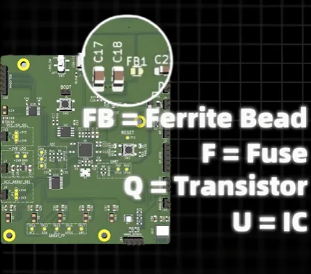
R marks resistors, including chip resistors, networks (sometimes RN), and potentiometers (sometimes RV or VR). C marks capacitors of every dielectric—ceramic, electrolytic, tantalum, film. L marks inductors and coils. F marks fuses. FB marks ferrite beads used for high-frequency noise suppression on power and USB rails.
Factory note: FB and L are not interchangeable in documentation even when both look like a dark chip inductor. Beads are selected for impedance at a frequency; power inductors are selected for inductance and saturation current. A swapped designator in the BOM sends the wrong reel to the SMT line.
Active Devices and Connectors: D, U, Q, SW, J, JP
D covers diodes, Schottky, Zener, and LEDs. U is the preferred prefix for ICs and other inseparable assemblies. Q covers bipolar transistors, MOSFETs, and most three-terminal discretes. SW marks switches. J marks connectors (jacks, headers, board-to-board). JP marks jumpers or solder-blob options.
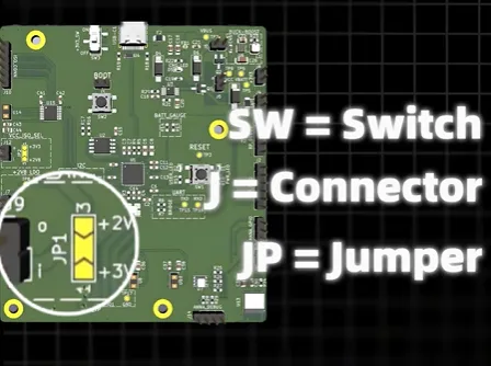
Polarity travels with these codes. D and LED cathode bars, U pin-1 dots or bevels, and Q pin-1 marks must sit next to the correct pad, not under the body. Reverse-inserted electrolytics, LEDs, and SOIC packages are among the highest-cost first-pass defects in mixed SMT/TH assembly.
Test and Timing Codes: TP and Y
TP marks a test point—a via, pad, or loop reserved for ICT, flying probe, or bench debug. Y marks a crystal or oscillator. Some libraries still use X or XTAL; freeze one convention in the schematic template before layout.
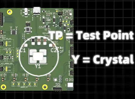
Keep TP designators on the finished board even when 0402 passives lose their letters. Test engineering and field service need a visible handle. Y parts are orientation-sensitive on some packages; pin-1 or pad-1 marks belong in the same legend pass as the designator.
| Prefix | Component class | What buyers and assemblers should verify |
|---|---|---|
| R | Resistor | Value and tolerance live in the BOM, not in the "R" code |
| C | Capacitor | Polarity mark required for electrolytic and tantalum |
| L | Inductor / coil | Do not confuse with FB on power-filter nets |
| D | Diode / LED | Cathode bar must clear the pad by ≥0.2 mm |
| U | IC / inseparable assembly | Pin-1 mark required; unique U# vs schematic |
| Q | Transistor / MOSFET | Pin-1 / tab orientation vs courtyard |
| F | Fuse | Rating and footprint in BOM; keep-out for replacement |
| FB | Ferrite bead | Impedance curve, not inductance, drives the MPN |
| SW | Switch | Actuator keep-out and orientation |
| J | Connector | Pin-1 and mating side; mechanical keep-out |
| JP | Jumper | Default open/short documented on assembly drawing |
| TP | Test point | Net name optional; designator mandatory for ICT |
| Y | Crystal / oscillator | Load-cap pair (C) must stay with the Y instance |
Why Reference Designators Matter in SMT Assembly and CAM Review
Pick-and-place machines treat designators as strings, not integers. R1 and R01 are two different locations. Duplicate U3 entries, missing C14, or a schematic that says IC1 while the Gerber says U1 will stop a PCB assembly quote in engineering review or throw a first-article discrepancy.
On the line, operators and AOI programs use the legend to confirm polarity after a nozzle dump or a reel splice. Medical and automotive builds add an extra constraint: the assembled board must remain traceable to the BOM revision. A missing or clipped designator on a polarized part is an IPC-A-610 process defect, not a cosmetic note.
CAM review at the fabricator is where many jobs stall. Legend drawn on pads, 0.6 mm characters that wash out, and notes that say "add standard marks" with no coordinates all generate engineering questions. Those holds delay copper and mask that were otherwise ready. Reserve keep-in zones for date codes, UL marks, and factory logos before you lock the courtyard map.
Application impact is consistent across automotive electronics PCB modules, industrial control PCB I/O cards, and consumer electronics PCB wearables: dense boards still need a human-readable index for debug. HDI and flex designs may drop outlines on 0201 parts, but connectors, fuses, crystals, and test points should keep their letters.
Silkscreen DFM Rules That Keep PCB Markings Readable After Fabrication
Readable codes are a process limit, not a CAD zoom setting. AIVON CAM and legend print typically need about 1.0 mm (40 mil) character height and 0.15 mm (6 mil) stroke as a practical floor; 1.27 mm height is preferred. Hairline logo strokes fail the same way tiny designators fail: incomplete characters after ink spread over solder-mask texture.
Keep legend off solderable copper. A working clearance is 0.2 mm (8 mil) from pad edges; IPC-2221-style keep-outs in the 0.13–0.20 mm range are the usual review target. Ink on a pad becomes a wetting defect and a pseudo-solder risk. Ink under an 0402 or 0201 body can lift one end during reflow and contribute to tombstoning. Drop outlines and designators under those packages; offset the text or use a grouped callout.
Typography: sans-serif only, two reading directions (left-to-right and bottom-to-top), bottom-side text mirrored in Gerber so it reads correctly after fab. White on green remains the highest-contrast default. Confirm LPI versus direct-legend capability with the fabricator before you freeze 0.8 mm text on an HDI prototype.
| Parameter | Practical target | Risk if violated |
|---|---|---|
| Character height | ≥1.0 mm; 1.27 mm preferred | Washed-out R/C/U codes after print |
| Stroke / line width | ≥0.15 mm (6 mil) | Broken letters, unreadable polarity bars |
| Silk-to-pad clearance | ≥0.2 mm (8 mil) | Ink in solder, poor wetting, AOI false fails |
| Text under 0402 / 0201 | Avoid; offset or omit | Tombstone fulcrum, hidden designator |
| Reading directions | 0° and 90° only | Slow assembly and inspection |
| Factory / UL / date marks | Reserved keep-in, defined string | CAM hold, wrong certification mark |
Release checklist: every designator unique; BOM, centroid, and silk use the same prefix convention; polarity and pin-1 marks adjacent to the correct pad; no silk on pads or via-in-pad openings; smallest character still complete at 1:1; notes name the exact factory marks, format, and coordinates. Then request an instant PCB quote or assembly quote with Gerber, BOM, and centroid attached.
FAQ
Q1: Do PCB markings have to match the BOM and pick-and-place file exactly?
A1: Yes. The designator is the join key across schematic, layout, BOM, and centroid. R1 in the BOM must be R1 on silk and in the PnP file. R1 versus R01, or U versus IC for the same part, is treated as two different locations by placement software and will fail first-article or ICT mapping.
Q2: What is the minimum silkscreen size so R1 and C2 stay readable after fabrication?
A2: Plan for 1.0 mm character height and 0.15 mm stroke as a manufacturing floor, with 1.27 mm height preferred. Text below about 0.6–0.8 mm often prints incomplete on standard LPI legend. Confirm the fabricator’s legend process (screen, LPI, or direct print) before you lock dense HDI designators.
Q3: Can I omit reference designators on 0402 and smaller parts to save space?
A3: You can omit outlines and body-centered text under 0402/0201 to reduce tombstone risk, but do not delete the identity of polarized parts, connectors, fuses, crystals, or test points. Offset those designators or group them in a readable callout block so assembly and service can still map the board to the BOM.
Q4: Is silkscreen on a pad only a cosmetic issue?
A4: No. Ink in a solderable opening interferes with wetting, changes joint appearance, and can fail AOI or IPC-A-610 workmanship. CAM will usually query clip/move/accept before tooling. Keep ≥0.2 mm clearance from pad edges.
Q5: Do flex, rigid-flex, and HDI boards use the same marking codes?
A5: Yes. R, C, U, Q, and the rest are schematic-class codes, independent of stack-up. What changes is print real estate: polyimide flex and HDI often need smaller or offset legend, and some marks move to a coverlay-safe zone. The prefix-and-number system stays the same.
Let's go through some common PCB markings.
R means resistor, while C means capacitor.
L stands for inductor, and D is used for diodes and LEDs.
U identifies an IC, while Q usually marks a transistor or MOSFET.
F means fuse, and FB stands for ferrite bead.
You'll also see SW for switches, J for connectors, and JP for jumpers.
TP marks a test point, while Y commonly identifies a crystal or oscillator.
And the number tells you which component it is.
So R1 means resistor number one, while C2 means capacitor number two.
Once you know these codes, reading a PCB gets much easier.





