










PCB Placement: Beginner Checklist Before Routing
What This Video Covers
Effective component placement is one of the most important steps in PCB design and directly determines routing success, manufacturing yield, and final product reliability. This video provides a practical beginner checklist to follow before drawing any traces.
The guide emphasizes grouping related components together — such as MCUs with their crystals and decoupling capacitors — to minimize trace lengths and improve signal integrity. It stresses placing connectors (USB, power inputs, headers) first to ensure accessibility and mechanical feasibility. Viewers learn why leaving adequate space between parts is essential for SMT assembly, inspection, and rework, preventing issues that look fine on screen but fail in production.
Finally, aligning similar components in the same orientation and direction simplifies automated assembly, visual inspection, and debugging. These foundational practices apply to FR4 PCB, Flexible PCB, HDI PCB, and multilayer designs across IoT devices, industrial control systems, medical equipment, and automotive electronics.
Implementing a solid placement strategy early prevents costly redesigns and supports smoother transition from PCB prototype to mass production.
Get an instant PCB quote for your next project or explore professional turnkey PCB assembly services and 4-layer PCB capabilities.
Key Highlights
- Group Functionally: Place related components (MCU, crystal, decoupling caps) close together to shorten traces and enhance signal integrity.
- Prioritize Connectors: Position USB, power, and header connectors first to ensure accessibility and mechanical fit.
- Assembly-Friendly Layout: Leave sufficient space and align similar components in the same direction for easier SMT assembly, inspection, and rework.
Why Component Placement Determines PCB Success
Component placement forms the foundation of any successful PCB layout. Poor placement decisions made early often lead to complex routing, increased layer count, signal integrity problems, and higher manufacturing costs. In production environments, boards with suboptimal placement frequently encounter issues during SMT assembly, AOI inspection, and functional testing, resulting in lower yields and delayed time-to-market.
From a CAM engineering perspective, well-placed components facilitate cleaner panelization, better fiducial marker utilization, and reduced risk of solder bridging or tombstoning. For multilayer and HDI designs, strategic placement also helps maintain controlled impedance routes and minimizes via usage, which directly impacts fabrication complexity and cost.
In flexible PCB applications, improper placement can cause excessive stress concentrations during bending, leading to trace fractures or component detachment over repeated flex cycles. Early attention to placement ensures compliance with DFM rules and supports high-reliability requirements in automotive, medical, and industrial applications.
Essential Grouping Strategies for Functional Blocks
Grouping functionally related components minimizes trace lengths, reduces parasitic inductance and capacitance, and improves overall electrical performance. For digital circuits, placing the MCU, its clock source (crystal or oscillator), and decoupling capacitors in close proximity is critical. This configuration shortens high-speed signal paths and provides effective noise suppression.
Analog sections, power management ICs with their inductors and capacitors, and interface circuits should each form their own logical clusters. In mixed-signal designs, maintaining physical separation between analog and digital domains while keeping internal groups tight helps prevent crosstalk and ground noise coupling.
Production data shows that boards following strong grouping principles achieve better first-pass yields during assembly and require fewer engineering questions (EQs) during CAM review. Proper grouping also simplifies thermal management by localizing heat-generating components and allowing more effective copper pour usage for heat dissipation.
Prioritizing Connectors and Mechanical Constraints
Connectors must be positioned first due to their mechanical and enclosure-related constraints. USB ports, power jacks, header arrays, and mounting holes dictate the overall board outline and internal component positioning. Placing them early prevents conflicts with other parts and ensures proper accessibility for cables and mating connectors in the final assembly.
In practice, overlooking connector placement often results in boards that cannot fit properly into enclosures or require awkward cable routing, increasing assembly labor and reliability risks. For edge-mounted connectors, clearance from board edges and V-CUT or scoring lines must also be verified during this stage.
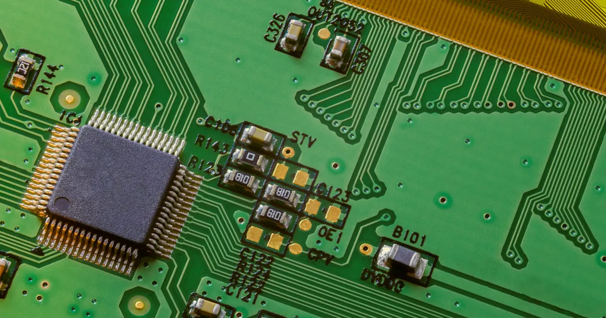
Assembly-Friendly Spacing and Orientation Rules
Adequate spacing between components is essential for reliable SMT assembly. Pick-and-place machines, solder paste printing, and reflow processes all require sufficient clearance. Components placed too closely increase the risk of solder bridges, insufficient solder joints, and difficulties during rework or inspection.
Aligning similar components (such as all 0805 resistors or all SOIC packages) in the same rotation direction significantly improves assembly efficiency and reduces feeder changeovers on SMT lines. Consistent orientation also aids visual inspection and debugging by creating predictable patterns on the assembled board.
Table: Recommended Minimum Clearances for Common Component Types
| Component Type | Minimum Spacing to Adjacent Parts | Rationale for Spacing |
|---|---|---|
| 0402 / 0603 Passives | 0.3 - 0.5 mm | Prevents solder bridging |
| 0805 / 1206 Passives | 0.5 - 0.8 mm | Allows rework and inspection |
| SOIC / QFN ICs | 0.5 - 1.0 mm | Accommodates thermal relief and AOI |
| Connectors/Headers | 1.0 - 2.0 mm | Ensures mechanical access and mating |
Common Placement Pitfalls and Real Manufacturing Failures
Common errors include placing decoupling capacitors too far from IC power pins, resulting in high-frequency noise issues that only appear during functional testing. Dense layouts without proper spacing often cause solder mask bridging or incomplete soldering in production, leading to intermittent failures and costly field returns.
In flexible circuits, placing components across bend areas without sufficient keep-out zones frequently causes cracking of solder joints after dynamic flexing. Multilayer boards with misaligned high-pin-count BGAs and connectors can create routing bottlenecks that force additional layers or compromised signal integrity.
Addressing these pitfalls early through systematic checklists dramatically reduces CAM engineering interventions, panelization problems, and overall production risks.
FAQ
Q1: Why is component placement more important than routing in PCB design?
A1: Poor placement creates routing nightmares, longer traces, signal integrity issues, and assembly problems that cannot be easily fixed later. Good placement sets the foundation for a clean, manufacturable board.
Q2: How much space should I leave between components for assembly?
A2: Leave enough clearance for soldering, inspection, and potential rework. Overly dense layouts that look good in CAD often cause defects during SMT assembly or increase manufacturing costs.
Q3: Should I place all connectors before other components?
A3: Yes. Connectors have mechanical and enclosure constraints. Placing them first prevents them from being blocked by other parts and ensures the overall layout remains practical.
Q4: How does component orientation affect SMT assembly yield?
A4: Consistent orientation of similar components reduces machine setup time, minimizes placement errors, and improves solder joint quality. Random orientations can lead to higher defect rates and slower production throughput.
Q5: What placement considerations are critical for flexible PCB designs?
A5: Avoid placing components across bend lines, maintain adequate keep-out zones for dynamic flex areas, and group components to minimize stress on solder joints. Proper placement significantly extends the flex life of FPC assemblies.
Before you start routing your PCB — stop.
Bad placement can ruin a board before a single trace is drawn.
One.Group related components
Start by keeping related components close.
MCU, crystal, decoupling caps — if they work together, they should sit together.
Two.Place connectors first
Look at your connectors. USB, headers, power inputs.
If connectors are blocked or hard to reach,the whole layout suffers.
Three.Leave space for assembly
Think about assembly.
Don't pack parts too tightly.
What looks fine on screen can fail during soldering.
Four.Align similar components
And finally, align similar components.
Same type, same direction.
It's easier to assemble, inspect, and debug.





