










Custom Tester PCB: 2-Layer DFM That Shipped 500 Solar HATs
Key Moment
- 0:00 Introduction
- 0:21 What's Inside the Test Fixture
- 0:47 ST-Link, Serial & Raspberry Pi Pico
- 1:08 Breakout Board & Voltage Measurements
- 1:33 Field-Style Power Testing
- 1:58 Test Harness & Bed of Nails
- 2:40 Resistance Checks
- 3:28 Analog Multiplexers
- 4:03 PCB Sponsorship
- 4:42 Programming the STM MCU
- 5:10 Running a Live Automated Test
- 5:37 MPPT Cycle & Timing Optimization
- 6:14 Production Line Update
- 6:39 Outro
Project Background
Five hundred solar power HATs do not leave a Melbourne bench because the schematic looked tidy. They leave because every board was programmed, every current-set resistor was audited, every rail was measured, and a short charge cycle was proven before the box was sealed. That is the production problem AutoEcology faced with the PV Pi, a Raspberry Pi HAT that takes a 12 V LiFePO4 pack and a solar panel on XT30 connectors, runs true MPPT on a TI BQ25756, talks UART from an STM32F103, and back-feeds 5 V into the 40-pin header.
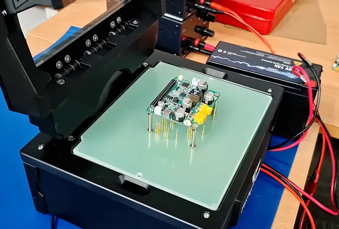
The market need is blunt. Off-grid Raspberry Pi deployments want a stout 5 V rail, a wide solar window, an RTC, a watchdog for a locked SBC, and a wake path when the pack is healthy. UART on pins 14 and 15 should report voltage and current the same way a customer will read it in the field. None of that survives a wrong sense resistor, an unflashed STM32, a lifted probe pad, or copper left on a routed edge.
Luke Ditria and Matt built the interesting half of that system: true MPPT, a current limit you can audit with a meter, UART a Pi can speak, and a fixture that pretends to be a solar panel. The remaining half is copper that does not invent failures. Both the product HAT and the tester board live on the same 2-layer FR-4 discipline—honest holes, matching mask, copper pulled off the router, and pads a pogo pin can hit five hundred times.
What This Video Covers
The video is a production-floor walkthrough, not a product teaser. Luke and Matt show the bed-of-nails fixture, the Pico-and-mux measurement path, the ST-Link programming step, and the limited supplies that stand in for a solar panel and pack.
Viewers see why a Raspberry Pi Pico cannot see fifteen or twenty nodes on its own ADC pins, and why two 16-channel muxes do the walking. They see resistance printed first—especially the programming resistor that sets charge current—then LED rails and feedback voltages. An ST-Link flashes the STM32 before USB-serial talks the same UART a customer will use. Supplies sit at 24 V, 20 V, and 12.5 V, each limited to 1 A. When Luke hits enter, resistances print, voltages print, 20 V comes up, and the charger hunts through an MPPT cycle.
The video also covers the timing tax. Early scripts used long settles. Five hundred and fifty boards will not wait thirty seconds each. The team trimmed waits until a comment could report about 23 seconds a board. Along the way they answer the questions production engineers actually ask: why so many test points, why the large SMD capacitors, why there is no 12 V pass-through, and why the tester PCB must be treated with the same 2-layer seriousness as the HAT it certifies.
Project Highlights and Key Features
- True MPPT on the TI BQ25756, charging a 12 V LiFePO4 pack at up to 10 A from a wide solar window, with UART telemetry on Raspberry Pi header pins 14 and 15.
- A second 2-layer FR-4 tester PCB that is a probe breakout plus Pico and muxes, not a one-off wiring harness.
- Bed-of-nails coverage: single-sided test pads 0.8–1.0 mm on a 1.27 mm or coarser grid, sized for pogo life over 500-plus cycles.
- Sense-resistor audit instead of a full 10 A station, so a wrong current-set part fails the script before it can become a hot field unit.
- ST-Link programming of the STM32F103 first, then USB-serial on the same UART a customer uses, so an unflashed MCU cannot masquerade as a solder defect.
- Simulated solar and pack rails at 24 V, 20 V, and 12.5 V, each current-limited to 1 A, with an MPPT hunt inside the 23-second window.
- Shared 2-layer FR-4 habits on both boards: 1.6 mm class, lead-free HASL on the tester (HASL or ENIG on the HAT), heavier copper in the HAT power path, no HDI, no buried vias, no impedance coupon.
- Power pours that stop about 0.2 mm before a routed outline and about 0.4 mm before a V-cut, so a 5 V plane does not become a burr after the router.
- Panel thinking for a 500-board run: named PTH versus NPTH, mouse-bite or stamp-hole tabs, large holes declared as drill or precision route, and mask that matches the quote.
Challenges Encountered During Development
The electrical challenge is coverage versus time. A 10 A solar HAT has to prove programming, current-set accuracy, rail health, and a short charge cycle in under half a minute. Muxes add settling you cannot afford at 23 seconds. A full-current pass needs headroom no 23-second station wants. Measuring the set resistor is safer; missing it ships either a polite brick or a hot one.
The firmware challenge looks like a manufacturing defect if you get the order wrong. An unflashed STM32 fails UART in a way that looks like a cold joint. Programming has to happen before the serial check, or the script will fail good copper.
The mechanical challenge is contact life. Five hundred boards means five hundred pogo cycles on the same pads. Pads smaller than about 0.8–1.0 mm, or pads buried under mask or ink, turn the fixture into a false-fail machine. Mixed via covering does the same: HASL fills a barrel you wanted tented, or a crown tip lands on solder mask instead of copper.
The CAM challenge is the quiet one. Quote says tented vias while the mask layer leaves windows. Silkscreen sits on an SMD pad. A mounting hole never declares PTH or NPTH. Copper kisses the outline. Those four mismatches are how a 5 V pour becomes a routed burr, how a pogo pad loses copper after the contour, and how a 40-pin header or XT30 shell fails to wet. A related 2-layer panel that measured 179 × 158.3 mm arrived as a customer 3×2 with V-cut, 4 mil pad-to-pad where 7–8 mil would have held a mask bridge, and features on the outline. After routing that is exposed copper and a ground a 10 A charger should not share with a probe.
Panelization at this quantity is not optional. Five hundred HATs do not travel as loose singles. They travel as panels that must survive HASL, flying probe, and a clean break. On another 2-layer FR-4 job—169 × 411.67 mm, sixty pieces, customer 1×4, V-groove, zero process edge—CAM stopped on holes larger than 3 mm and connection tabs with no stamp holes. Past about 3 mm a drill wanders, the hole goes oval, and a locating pin no longer matches the fixture plate. Tabs without mouse bites or stamp holes (0.8–1.0 mm on a 1.5–2.0 mm pitch) snap with micro-cracks. M2.5 HAT holes can stay drilled. Anything that looks like a slot, a tool hole, or a fat NPTH on the tester panel has to be named: drill or route.
Cost and timeline sit on top of all of that. A 10 A production station is expensive. Extra layers and HDI would not have fixed sense accuracy or pogo life. The boards only needed to be dull and correct—and they needed to arrive with the same registration, annular ring, and mask rule on board 400 that they had on board 1.
How AIVON PCB Helps
AIVON's job on a run like this is not to redesign the PV Pi. It is to make both the product board and the tester board boring enough that a 23-second script can be trusted. A tester with lifted probe pads is a false-fail machine. A HAT with copper on the routed edge is a field return that looks like firmware.
On boards like these we start with the stackup nobody needs to overbuy. Two-layer FR-4, 1.6 mm class, lead-free HASL unless first article argues for ENIG, heavier copper in the charger path so a 10 A peak does not live in a hairline trace. No impedance coupon. No buried vias. The manufacturing value is registration, annular ring, and mask that matches the order note. Drill that lands in the 40-pin header and the XT30 shells is what lets the HAT seat on a Pi and still wet on the fixture. Open every PTH the assembler or the pogo needs. Tent only where the Gerber mask and the quote say the same thing. Pour enough power copper for the bulk capacitors people comment on, then stop that pour about 0.2 mm before a routed outline—0.4 mm if the panel uses V-cut.
That last sentence is the same review we run when a 2-layer file hits CAM. Quote says tented, mask layer leaves windows; silkscreen sits on an SMD pad; a mounting hole never declares PTH or NPTH; copper kisses the outline. We ask the question before the panel ships, then edit the mask or the pour so the fixture sees the pad the designer drew.
Panelization is the other half of custom work at this size. We treat large holes as a named process: drill or precision route. We put a standard stamp-hole pattern on tabs unless the customer writes that they will route solid tabs themselves. We keep M2.5 HAT holes drilled and force a decision on slots and fat NPTH on the tester panel. That is how board 400 matches board 1, and how Matt's mux scan measures a resistor rather than a ragged edge.
The DFM checklist that falls out of this video is specific to a power HAT plus a bed-of-nails tester:
- Test pads at least 0.8–1.0 mm, on at least 1.27 mm centres, mask-open so the crown tip hits copper.
- Copper at least 0.2 mm from a routed outline and 0.4 mm from a V-cut.
- Pad-to-pad at least 7–8 mil where the mask must bridge in dense sense and mux neighborhoods.
- One tenting rule in both the quote and the solder-mask layer.
- PTH versus NPTH named; mask open on headers and XT30.
- Sense resistor on a two-wire pad so the 10 A set point can be audited without a 10 A fixture.
- Ceramics on the BQ25756 and STM32 rails so an MPPT hunt does not look like a void.
AIVON PCB pairs that review with rapid PCB manufacturing and fast-turn 2-layer capacity. Prototype iterations on the tester can move while the product HAT panel is still in CAM. Expert DFM analysis is the difference between a fixture that stays honest after 500 cycles and a fixture that starts failing good boards. Quality is not a slogan here; it is whether the pogo still sees copper, whether the 40-pin header still wets, and whether the outline still matches the plate. Reliable delivery is what lets a Kickstarter-scale HAT run keep a 23-second station fed. One-stop PCB prototyping and production means the same shop that holds the 2-layer EQ queue can also speak to assembly notes on headers, XT30 shells, and programming pads.
That combination—standard 2-layer stackup, aggressive CAM questions, panel rules that survive HASL and breakout, and a DFM pass aimed at pogo life—is how custom tester PCB work becomes a production asset instead of a second source of defects.
Conclusion
AutoEcology's story is a maker brief that grew a production problem and a 23-second cycle. Luke and Matt solved the interesting half in the video: MPPT, UART, a fixture that pretends to be a panel, and a script short enough to ship five hundred boards. The 2-layer boards only have to be dull and correct.
If a power HAT now has a purchase order attached, put the test pads on one side, name the holes, pull copper off the outline, and treat the tester PCB like the product. Watch how that discipline looks on the bench in Luke Ditria's production test video, then read the manufacturing notes in Custom Tester PCB Work That Let AutoEcology Ship 500 PV Pi HATs.
Ready to put the same 2-layer FR-4 discipline under your next power HAT or bed-of-nails fixture? Request a quote from AIVON PCB, get a free DFM analysis on your Gerbers, and start the project with pads, mask, and outline rules a 23-second script can trust.
FAQ
Q1: What 2-layer stackup is enough for a 10 A MPPT Raspberry Pi HAT and its tester?
A1: Two-layer FR-4, 1.6 mm class, extra copper in the HAT power path, short sense runs, and ceramics on the charger and MCU rails. The tester can stay at 1 oz and lead-free HASL. Neither board needs HDI if current loops, annular rings, and pogo pads are correct.
Q2: Why measure the charge-current set resistor instead of running a 10 A functional pass?
A2: A full-current station needs headroom you will not want on a 23-second line. The programming resistor is the defect that would make that test dangerous or meaningless. A two-wire pad lets the script fail a wrong value before power is applied.
Q3: How should test pads be designed so a bed-of-nails fixture survives 500-plus cycles?
A3: Use single-sided pads 0.8–1.0 mm on a 1.27 mm or coarser grid, keep them open in the mask, and run a contact check before a voltage check. Mixed tenting or silkscreen on the pad is how a pogo starts landing on ink instead of copper.
Q4: How close can copper and test pads sit to a HAT or tester outline?
A4: Keep copper at least 0.2 mm from a routed edge and about 0.4 mm from a V-cut. Pull features 0.3–0.5 mm off the contour so a 5 V pour does not become exposed copper after the router.
Q5: Should tester vias be tented on HASL 2-layer FR-4?
A5: Pick one rule and put it in both the quote and the solder-mask layer. Mixed files are how HASL fills a barrel you wanted closed and how 2-layer jobs sit in EQ instead of moving to fab.
In our previous video, we talked about our test fixture and how we're using it to interface with the test points on the back of the PV Pi so that we can program and test the PV Pis before shipment. I'm joined again by Matt who's going to talk us through how you automate the testing of over 500 PCBs. So, without further ado, let's jump right in.
All right, so we'll pick up where we left off last time.
We talked last time a lot about this fixture and how it interfaces with the PV Pi through all these probe connections.
Yeah.
But I think we had some questions last time about what's inside the fixture and how that actually works.
What's inside the box? There is a few things that make the magic happen.
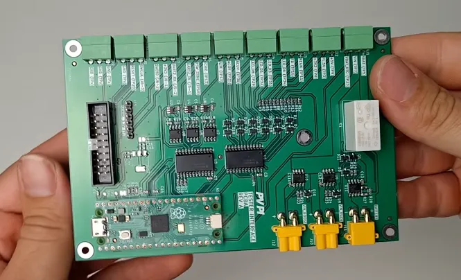
We can see all these wires and they're coming down from the test points that we just talked about. We have a few other things. So, we've got our ST-Link which is used for programming the MCU on the PV Pi. We also have a USB-to-serial converter as well as quite critically the Raspberry Pi Picos. So, this is kind of the brains of the operation and is what does all our code, our programming. And then that's essentially hooked up to a couple of power supplies and a battery. And this board here essentially breaks out the Pico Pi's connections and does all sorts of voltage measurements and control of different inputs.
Basically, this little setup here we're testing a whole bunch of things, but we've also got it kind of set up in a lab testing way as if it was out in the field. So, we're going to be probing it at a bunch of different points in the circuit and then we're doing some basic testing on the hardware, but then we're going to pretend it's out in the field.
Yeah.
We've got some different power supplies that were set to different voltages that's all the basic functionality still working.
Yeah, exactly. Essentially like turning on input voltages like they're a solar panel and charging a battery as a critical one obviously, but you know, talking over the serial communication exactly how you'll be talking to your PV Pis, kind of just emphasizing all the key functionalities on the board to make sure it's all working correctly before we ship them out to you guys.
All right, so talk me through a bit about exactly what this is doing. So, we looked and we saw that, you know, we're basically probing the circuit at different locations on the PV Pi. So, we're basically wired in via this test harness here.
That's correct. So, we have this big test harness coming up to this bed of nails that our board sits on there. That runs us down to this set of connectors on this board. And then, essentially, we're probing all of those different points on the board.
You can see the LED voltages.
Yeah, yeah, exactly. You know, your classic voltage rails, things like that. This board takes care of doing all those measurements. We've got pretty good coverage on this board, so we wouldn't expect much to fail.
I can see we've got quite a lot of wires here. What other sort of testing are we doing?
There's a good amount that's kind of... Actually, maybe we'll step back to the start. So, some of the measurements we take at the start, like resistance measurements. So, these are about checking resistors on the board that are really critical to the design. Take for example, there's a resistor on there that sets the maximum charge current that this board can output. So, if that was set too low or too high, a manufacturer accidentally added a wrong resistor, you'd either have a product that doesn't work at high charge rates or would operate too high and potentially damage itself.
Right.
You could kind of design a fixture, it would be quite complicated to run at those maximum charge currents and functionally check that, but just practically, it's quite a difficult design. So, there's some cases where we're doing resistance measurements to check those kind of things. So, you can see on the board here the Pi Pico only has so many ADC inputs. I think it's got about three, whereas we need I think we're using about 15 or 20.
Right.
The easy way to do that is using these here, which are called an analog multiplexer. So, essentially, it's got 16 channels a piece. And then, with just a couple of GPIOs from the Pi Pico, we can change to the different channels we want. So, we could select the feedback voltage or the LED voltages. And they kind of correlate to points on the board. We select them, feed them into the ADC on the Pi Pico, and then just read that voltage back.
While we're on the topic of our tester PCB, I'd like to stop and thank our PCB sponsor, JLCPCB, who manufactured the PV Pi test board. And right now, JLCPCB offers up to $60 off new users when they get their first PCB prototype manufactured. JLCPCB is a one-stop PCB manufacturing and assembly supplier. Simply upload your Gerber files and your assembly instructions and JLCPCB will do the rest. As I said, JLCPCB manufactured and assembled our PV Pi tester and they did a great job. And this is the PCB we'll be using throughout our production run. So, thanks to JLCPCB for sponsoring this video and let's get back to the main video.
Okay, so we're probing the different voltages, measuring things like resistors, outputs, kind of charging the battery at one point, I think, inputs. Before all that though, we have to program.
Yeah, this is true. So, the other side, what will kind of happen is there's resistance measurements, the voltage measurements. The next thing is to program the board. So, on the board we have a little STM microcontroller. So, we make connection to these pins here, which is the programming interface. And we essentially just hook that into an ST-Link and then we have a bit of an automated program running to load the firmware files on there.
We've got it set up now and I'll turn this one on. So, we've got our 24 V, 20 V and our 20 V and our 12.5 V both set to 1 amp hooked up over there. And we're ready to go to run our test. I press enter. First thing that happens is we get some resistance readouts and then we're going through and reading some voltages. Now, what's happening is we're drawing 1 amp at 20 V. Sorry, it just flicked off because it finished that test. We'll probably be about to see this one go though. So, this one's just running that. Does a little MPPT cycle, which is why we saw the voltage come down there. Sets to the max current. There's still some values in here. They are mostly to do with timing and getting... So, I talked to Luke this before. Getting kind of the MPPT cycle and timing to line up. There's a big art in this kind of testing to timing where if you had all the time in the world, you'd just set, you know, 20, 30 seconds delays, let it all settle, and it'll be fine. Having to test 550 of these, we just want to keep that test time to an absolute minimum. So, trying to work out ways to optimize that timing.
So, you're saying like we switch on the power supply, we've got to wait for everything to settle before we take a reading.
Yeah.
All right. Oh, cool. So, we'll eventually have a whole production line here. We've got a beam set up as well. We're just waiting on the actual boards at the moment.
Yes.
So, they're currently being manufactured. We've got all our... I'm just like, almost 700 cables. We've got all the kits of parts as well. The boxes as well.
And yeah, so it's all happening.
Yep. We're waiting. Ready to go.
Yeah, exciting day.
Indeed.
Yeah. So, thanks for watching. We hope you enjoyed that little behind-the-scenes look. We'll be putting out another video when we get our first full production batch, and we'll take you through our process and our packaging and shipping of the boards. There was a small delay in the manufacturing as we were unable to get the bare PCBs finished before the Lunar New Year, which then delayed the assembly process. But, we're only about a week or two behind schedule, and still should get everything done by our original timeline.
So, thanks for watching, and I'll see you in the next one.





