










SMD Component Removal: Professional PCB Rework and Repair Techniques
What This Video Covers
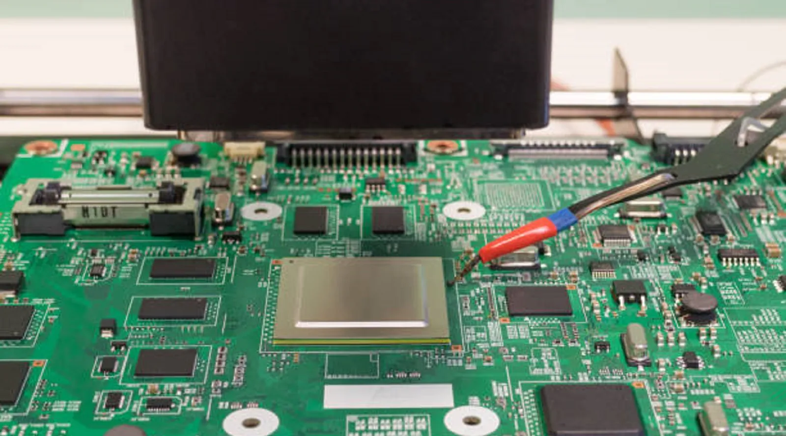
This video demonstrates industry-standard SMD component removal processes essential for PCB rework, repair, and prototype modification. It explains safe desoldering techniques using hot-air stations, soldering irons, and specialized tools to remove surface-mount devices without damaging pads, traces, or underlying layers.
Key engineering considerations include thermal profiling, component handling on dense HDI and multilayer boards, and post-removal inspection to maintain signal integrity and long-term reliability. The content is highly relevant for OEM engineers and repair teams working with high-value assemblies in aerospace, automotive electronics, medical devices, and industrial control systems.
For pricing on rework services or new assemblies, request an instant PCB assembly quote or review full PCB assembly services.
Key Highlights
- Precise thermal control during SMD removal prevents pad lifting, delamination, and damage to multilayer or HDI PCB structures while preserving signal integrity.
- Professional desoldering techniques enable reliable component replacement on complex boards used in mission-critical aerospace, automotive, and medical applications.
- Proper SMD removal and inspection procedures support high-yield rework, reducing scrap and extending the service life of industrial and IoT electronics.
Common Manufacturing Challenges in SMD Desoldering
SMD component removal on modern PCBs presents several production challenges, particularly with high-density interconnect (HDI) and multilayer constructions common in compact electronics. Excessive localized heating can cause copper pad detachment, via damage, or substrate delamination, especially on boards with thin dielectrics or heavy copper planes that act as heat sinks.
Mechanical stress during component lifting often results in trace fractures or micro-cracks in vias that may only manifest as intermittent failures during thermal cycling or vibration testing. In lead-free assemblies, higher melting temperatures exacerbate these risks, requiring tighter process windows.
Real-world production data shows that improper technique frequently leads to increased scrap rates in aerospace and medical device rework, where traceability and zero-defect standards are mandatory. Mitigation involves pre-heating the entire board area, using appropriate flux formulations to lower effective solder melting points, and employing vacuum pickup tools to minimize force.
Thermal Management and DFM Best Practices for Safe Removal
Effective thermal management forms the foundation of reliable SMD component removal. Hot-air rework stations with programmable temperature and airflow profiles allow operators to follow manufacturer-recommended reflow profiles adapted for removal, typically maintaining nozzle temperatures between 300–380°C for lead-free solder while monitoring board temperature to stay below glass transition thresholds.
DFM principles recommend designing component footprints with adequate pad extensions and thermal relief connections to large copper areas. This facilitates heat distribution and reduces the risk of pad lifting during rework. For dense HDI boards, staggered via placement and proper copper balancing across layers help maintain structural integrity.
Practical recommendations include applying no-clean or water-soluble flux prior to heating to improve solder flow and heat transfer. Technicians should use preheated boards (typically 100–150°C) to reduce thermal shock. Specialized tools such as heated tweezers or low-temperature desoldering alloys can further protect sensitive components and fine-pitch devices. Failure to observe these practices often results in hidden damage that compromises reliability in automotive under-hood or medical implant-adjacent applications.
Comparison of SMD Removal Methods
| Method | Typical Temperature | Best Applications | Key Advantages | Primary Risks |
|---|---|---|---|---|
| Hot-Air Rework | 300–380°C | Fine-pitch QFN, BGA, dense arrays | Uniform heating, minimal contact | Overheating adjacent components |
| Soldering Iron | 320–400°C | Larger resistors, capacitors | Low cost, precise tip control | Pad lifting on small footprints |
| Infrared/Preheater | 250–350°C | Large boards, rework preparation | Even heat distribution | Longer cycle times, potential warping |
Post-Removal Inspection and Quality Assurance Procedures
Post-removal inspection is critical to verify board integrity after SMD component removal. Visual inspection under magnification (10–30x) identifies lifted pads, solder bridges, or residue, while automated optical inspection (AOI) systems provide consistent detection of surface anomalies.
Electrical testing, including in-circuit and flying probe methods, confirms continuity and isolation of affected nets. For high-reliability applications, X-ray inspection reveals hidden via or internal layer damage not visible on the surface. Thermal imaging during powered functional testing can expose latent defects caused by micro-cracks.
Documentation of removal parameters (temperature profiles, tool settings, operator ID) supports traceability requirements in aerospace and medical sectors. Implementing these procedures minimizes field failures and supports continuous process improvement in PCB manufacturing and repair operations.
FAQ
Q1: How does improper SMD component removal affect multilayer and HDI PCB reliability?
A1: Excessive heat or mechanical stress can lift pads, damage vias, or cause delamination, leading to open circuits, reduced signal integrity, and premature failure in high-density designs.
Q2: What equipment and techniques are recommended for safe SMD removal on production PCBs?
A2: Hot-air rework stations with precise temperature and airflow control, combined with flux application and low-force component lifting, are standard for protecting board integrity during removal.
Q3: Which industries require documented SMD removal and rework procedures for PCB assemblies?
A3: Aerospace, automotive electronics, medical devices, and industrial control systems demand strict rework protocols to maintain compliance, traceability, and long-term reliability.
Q4: What DFM considerations help facilitate easier and safer SMD component removal?
A4: Incorporating thermal reliefs on pads, providing adequate spacing around critical components, and balancing copper distribution across layers significantly reduce rework risks and improve success rates during repair operations.
Q5: How can manufacturers minimize solder joint defects after SMD component replacement?
A5: Thorough cleaning of residual flux and old solder, precise paste or wire application, and controlled reflow profiling aligned with the original manufacturing process help ensure reliable new joints with proper fillet formation and minimal voiding.
Welcome to AIVON PCB. Today we're demonstrating professional SMD component removal. We start by applying flux to protect the pads and ensure smooth heat transfer. Using a hot air rework station with precise temperature control, we gently heat the component until the solder fully melts. Then, with steady hands, we carefully lift the component away, leaving the pads clean and undamaged. Perfect removal done right — no lifted pads, no bridges. What problem should we fix next? Let us know in the comments and follow AIVON for more soldering tips and PCB repair tutorials!





