02:50
02:50
Solder Mask Tenting
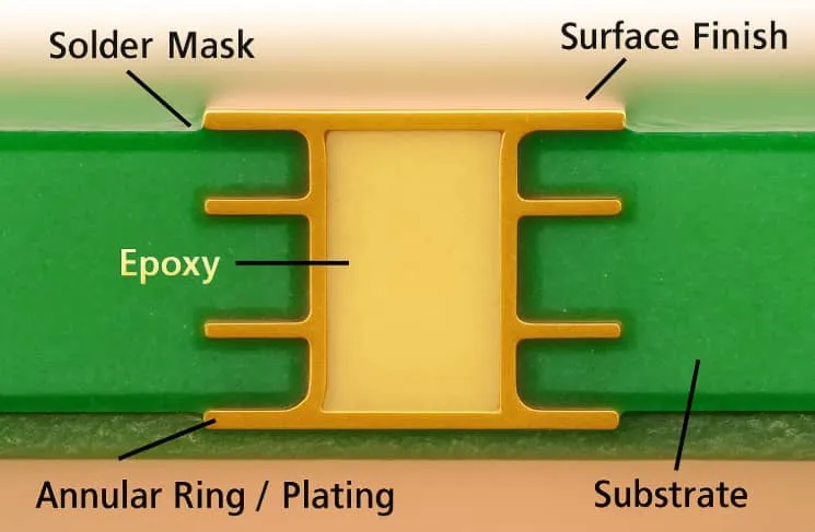
Solder mask tenting plays a crucial role in printed circuit board (PCB) design and manufacturing, serving as a protective technique to cover vias and through-holes with solder mask material. This method prevents solder from bridging or flowing into unintended areas during the assembly process, which can lead to short circuits, reduced reliability, or assembly defects. For engineers, designers, and hobbyists searching for information on solder mask tenting, this tag aggregates articles that delve into its implementation, benefits, and potential pitfalls, helping you optimize your PCB layouts for better performance and manufacturability. In practice, solder mask tenting is particularly valuable in high-density boards where space constraints demand precise control over solder flow. By fully encapsulating vias, it enhances insulation, protects against environmental contaminants like dust or moisture, and improves overall board aesthetics. Key considerations include selecting the appropriate solder mask thickness, ensuring compatibility with via sizes, and adhering to design rules that align with your fabrication partner's capabilities. For instance, tenting small vias can minimize signal interference in RF applications, while in power electronics, it helps maintain thermal integrity by preventing solder wicking. Understanding when to apply solder mask tenting versus leaving vias exposed can significantly impact your project's success. Articles under this tag explore real-world examples, such as troubleshooting common issues like incomplete tenting or mask peeling, and offer guidelines for tools like Gerber file generation to achieve reliable results. Whether you are refining a prototype or scaling production, these resources provide practical strategies to integrate tenting effectively into your workflow. For deeper insights into related PCB protection techniques, browsing connected topics can further enhance your design expertise.
Video Guide
-
02:50
Technical Articles
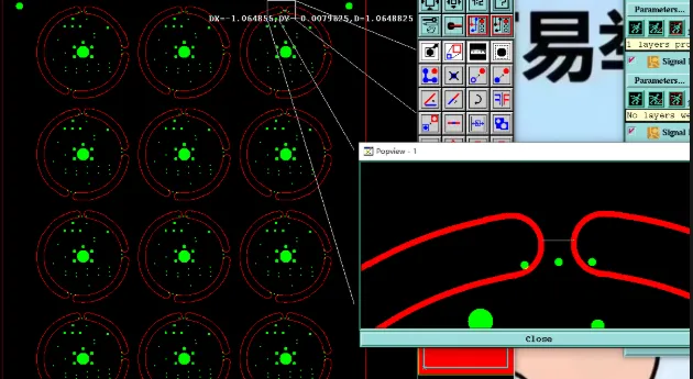
Undersized Panel Connection Tabs Risk Board Breakage in 2-Layer PCB
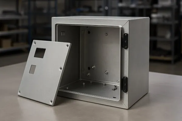
Common Sheet Metal Design Mistakes for PCB Enclosures
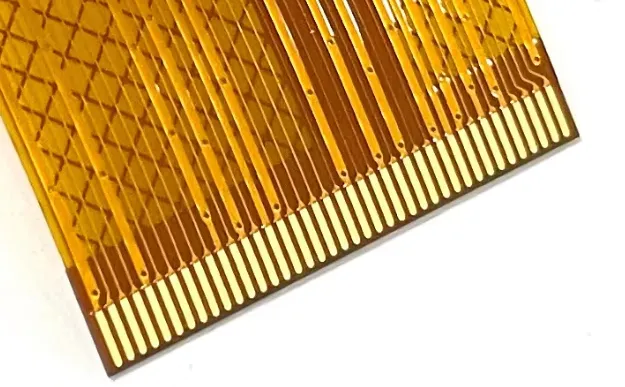
Should Via Openings Be Kept on FPC Boards?
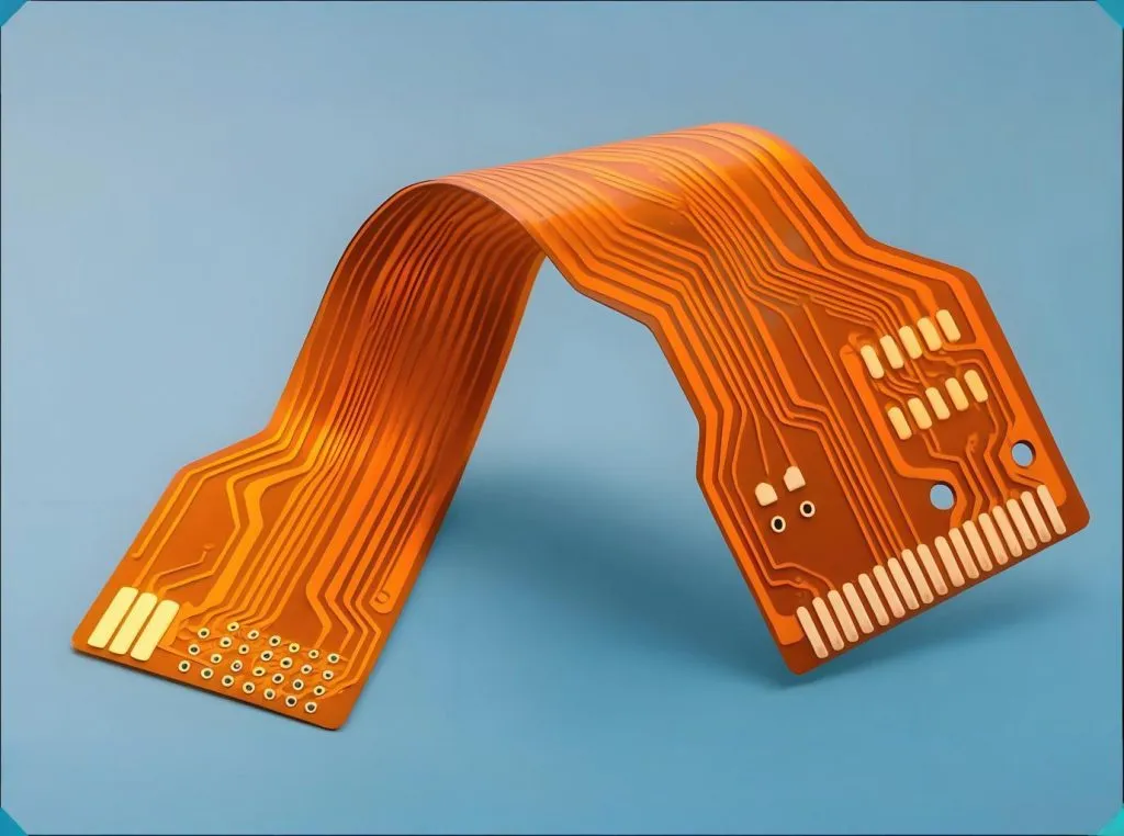
Canceling Via Openings on FPC to Prevent Long-term Oxidation
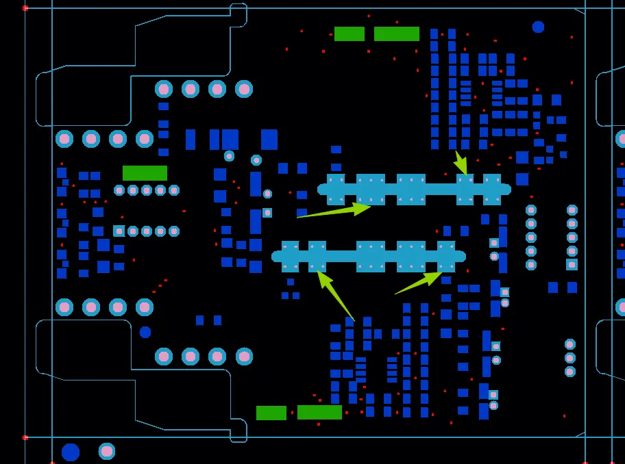
How DFM Review Prevented Via Reliability Risks in a 2-Layer FR4 PCB
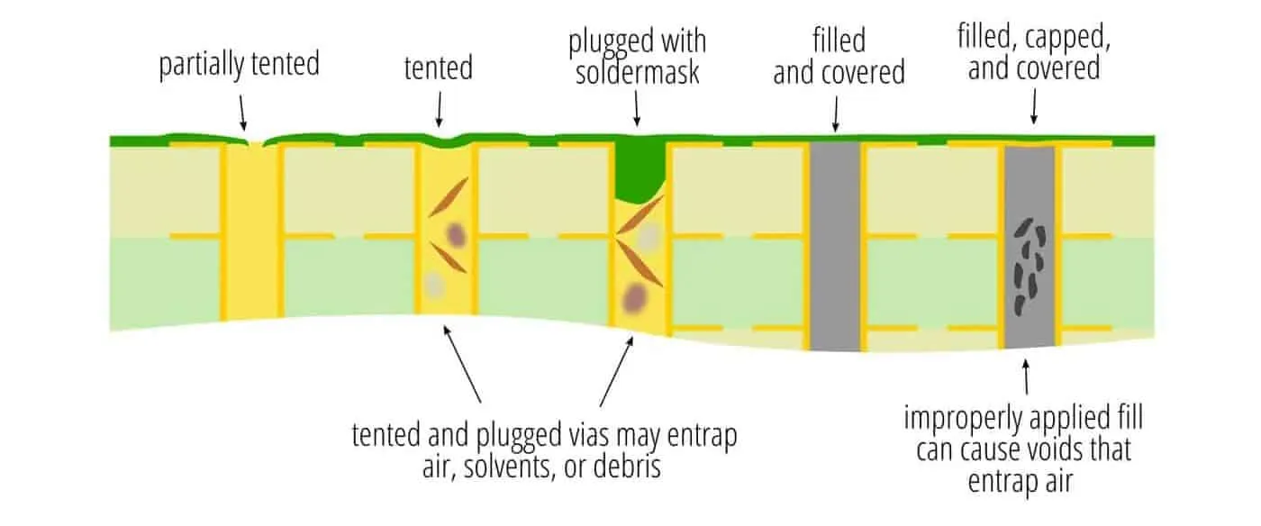
Overcoming Solder Wicking in Via in Pad: Techniques and Solutions
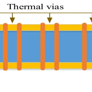
FR4 PCB Thermal Vias: Placement and Design Guidelines
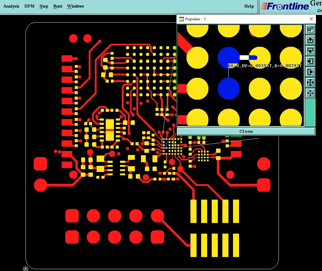
PCB Solder Mask and Via Design Issues: What CAM Review Commonly Finds
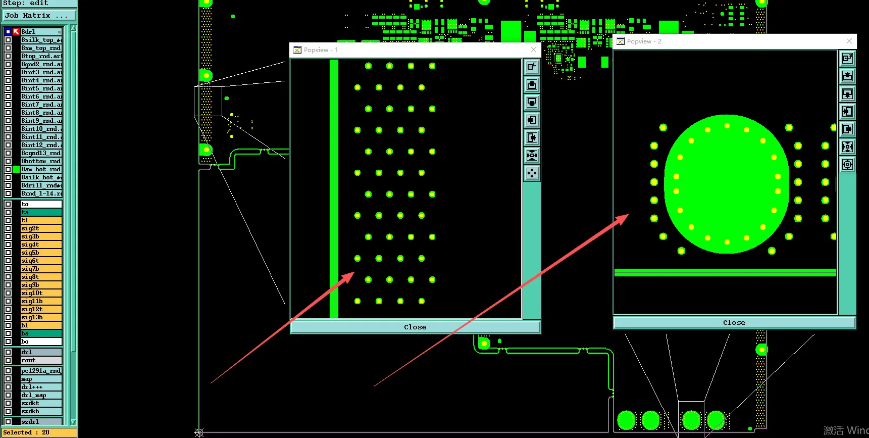
How We Resolved Resin Plug Tenting Conflict on 14-Layer PCB
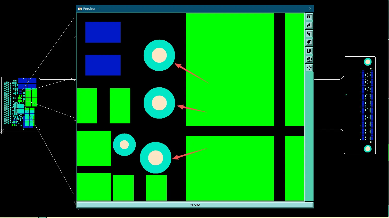
How CAM Review Fixed Stackup, Via Tenting & Outgassing Conflicts on a 7-Layer Rigid-Flex PCB
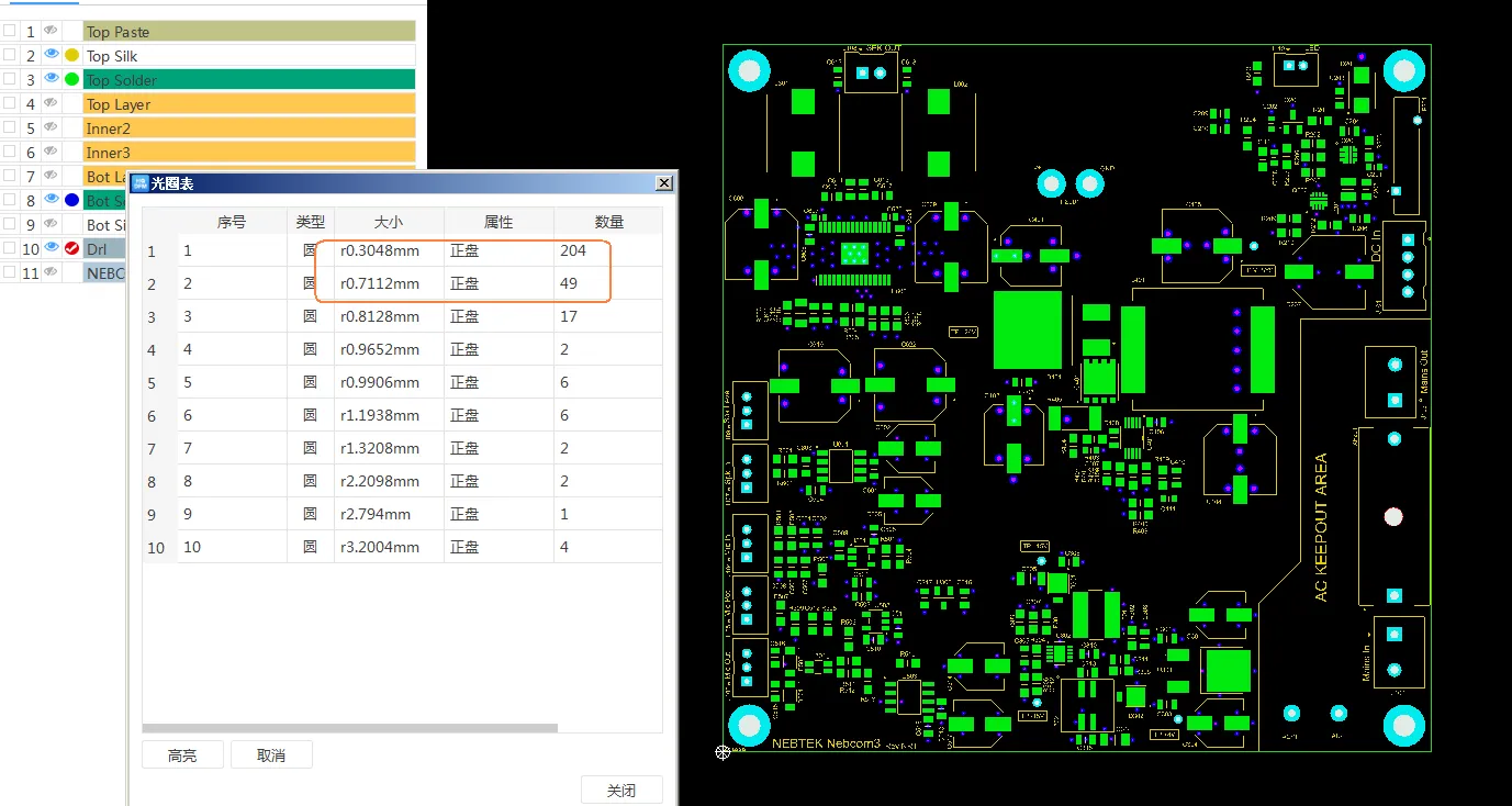
How DFM Prevented Via Tenting Issues in 4-Layer FR4 PCB
How to Avoid Solder Mask Issues Around HDI Microvias