










-
 00:58
00:58
What Is an HDI PCB? High Density Interconnect Explained
This video explains High-Density Interconnect (HDI) PCB technology and how it enables designers to maximize circuit density, miniaturization, and electrical performance in modern electronic devices. It explores key HDI features such as microvias, fine-line routing, and advanced multilayer stack-ups that allow more functionality to be integrated into smaller, thinner circuit boards. The video highlights how HDI designs improve signal integrity, reduce parasitic effects, and support high pin-count components by shortening routing paths and increasing interconnection density.
-
 00:58
00:58
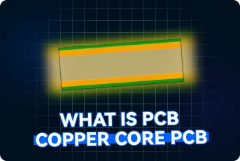
What Is a Copper Core PCB? Heavy Power and Heat Management Explained
This video explains copper core PCBs, a specialized PCB technology engineered for applications with extreme thermal and power requirements. It details the three-layer construction consisting of a copper circuit layer, an insulating dielectric layer, and a solid copper base that provides exceptional heat dissipation and high-current carrying capability. The video discusses how copper core PCBs help maintain reliability in demanding environments by efficiently managing heat and reducing temperature rise under heavy electrical loads. It also explores common applications such as power modules, motor drives, industrial converters, and other high-power systems, while comparing copper core PCBs with alternative thermal management solutions like aluminum PCBs and heavy copper PCBs to help engineers select the most suitable design approach.
-
 00:58
00:58
How Aluminum PCBs Move Heat Straight Down
This video introduces aluminum PCBs (metal core PCBs) and explains how their unique structure provides superior thermal management for high-power electronic applications. It covers the three-layer construction—copper circuit layer, thermally conductive dielectric, and aluminum base—and shows how this design efficiently transfers and dissipates heat, reducing hotspots and improving reliability. The video also explores common applications of aluminum PCBs in LED lighting, power supplies, automotive electronics, and industrial equipment, highlighting their advantages over conventional FR4 boards in thermal-critical designs.
-
 00:59
00:59
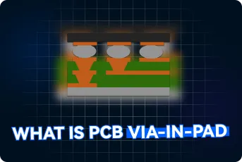
Via-in-Pad for BGA PCBs: When to Use It and Critical DFM Rules
This video provides a practical overview of Via-in-Pad (VIP) technology, a PCB design technique that places vias directly within component pads to overcome routing limitations in high-density layouts, particularly beneath fine-pitch BGA packages. It explains how Via-in-Pad improves routing density, shortens signal paths for enhanced high-speed performance, and facilitates efficient thermal transfer through the PCB stackup.
-
 01:00
01:00
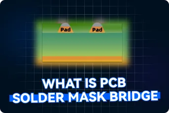
Solder Mask Bridge in PCB Manufacturing: Preventing Shorts in Fine-Pitch Designs
This video explains the role of solder mask bridges on PCBs and how they prevent solder bridging between adjacent pads during reflow assembly. It describes how the narrow solder mask dam acts as an insulating barrier that improves assembly reliability and reduces the risk of short circuits. The video also outlines the key design factors that determine minimum bridge width, including fabrication tolerance, solder mask material and color, copper thickness, and pad spacing. It emphasizes the importance of defining proper DRC rules early in the design process and carefully reviewing solder mask Gerber files before manufacturing, particularly for fine-pitch components such as BGAs and QFNs in HDI and multilayer PCB designs. These best practices help ensure smooth transition from prototype to mass production while minimizing assembly defects.


