










-
 00:59
00:59
Castellated Holes on PCBs — How Half-Holes Really Work
This video introduces castellated holes (castellations or half-holes) and explains how they enable direct board-to-board soldering for compact, modular PCB designs. It details the manufacturing process, where plated through-holes are created first and then precisely edge-milled to form semi-circular pads for strong electrical and mechanical connection between stacked boards. The video also highlights key design rules such as minimum hole diameter, pad spacing, and accurate alignment with the board edge to ensure reliable solder joints. It further discusses common failure risks like misalignment, weak plating, and thermal stress, and shows how properly designed castellations improve assembly efficiency and durability in applications such as IoT modules, wireless communication devices, industrial systems, and consumer electronics.
-
 01:02
01:02
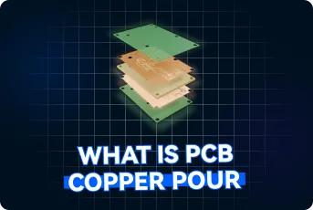
PCB Copper Pours: Critical Role in Modern PCB Design and Manufacturing
This video explains the role of copper pours in PCB design and how they improve electrical, thermal, and mechanical performance. It shows how continuous copper areas create low-impedance ground paths that enhance signal stability, simplify routing, and reduce noise. The video also highlights important design considerations such as controlling copper placement under pads, maintaining clearance for RF-sensitive areas, and avoiding issues that can affect soldering or antenna performance. It further compares copper pour strategies in 2-layer and multilayer PCBs, including optimal ground distribution for analog and digital circuits, with special focus on high-frequency designs that may require separated ground regions. Practical guidelines are provided for balancing heat dissipation, EMI reduction, and long-term reliability in complex PCB applications such as 4-layer, high-frequency, and heavy copper boards.
-
 00:57
00:57
Tented vs Untented Vias — Why It Matters for Reliability
This video explains the differences between tented and untented vias and how via treatment choices affect PCB assembly quality, reliability, and long-term durability. It describes how tented vias are covered with solder mask to prevent solder wicking during SMT assembly, reduce oxidation, and improve protection in high-density PCB designs. The video also discusses the potential risks of poor solder mask coverage, including cracking and flux entrapment. In contrast, untented vias are shown as beneficial for thermal dissipation, electrical probing, and certain high-current applications, though they may increase the risk of solder defects and environmental corrosion. Practical design guidelines are provided for selecting the appropriate via treatment in aerospace, medical, automotive, and other high-reliability electronic applications where PCB manufacturing precision is critical.
-
 00:52
00:52
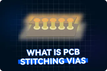
Stitching Vias in PCB Design: Essential for EMI Reduction, Heat Management & Signal Integrity
This video explains the function of stitching vias in PCB design and how they improve signal integrity, EMI control, and thermal performance in high-speed and RF applications. It describes how stitching vias create low-impedance return paths between ground planes and copper pours, helping contain electromagnetic interference and stabilize high-frequency signals. The video also covers recommended via spacing strategies for RF traces, power planes, and thermal management applications, while warning against common design issues such as isolated copper islands and unintended current loops caused by excessive via placement. Real-world examples demonstrate the importance of stitching vias in multilayer and rigid-flex PCB designs where controlled impedance, noise reduction, and efficient heat dissipation are essential.
-
 01:09
01:09
How Signals Jump Between PCB Layers: Vias Explained
How do signals navigate the complex, vertical maze of a multilayer PCB? The answer lies in vias—the essential bridges between layers. From the cost-effective through-hole via to the high-precision microvias used in HDI designs, each type carries unique trade-offs in signal integrity, routing density, and manufacturing cost. In this guide, we break down the mechanics of blind, buried, and laser-drilled vias to help you optimize your high-speed projects. Learn how to choose the right interconnection to boost reliability without overstretching your production budget.


