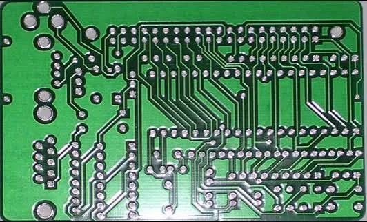
Most signal integrity failures on FR4 boards do not start with the trace geometry. They start with the return path. When a high-speed signal changes layers, the return current has to follow. If the nearest ground via is too far away, the current loops out across the plane, inductance jumps, and the edge rate pays the price.
That is the core of FR4 PCB ground via placement. Not "add some ground vias somewhere." Place them so the return path stays short and continuous.
Why Ground Vias Exist in the First Place
A ground via is not a stitching decoration. It is the vertical path that lets return current move between reference planes when the signal does the same.
On a multi-layer FR4 stack-up the signal may travel on L1, drop to L3, then come back up. Every time it transitions, the return current must also transition. Without a nearby ground via the return has to travel laterally across the plane until it finds one. That lateral travel creates a loop. Loop inductance rises. The via itself starts looking like a series inductor in the return path.
At a few hundred megahertz the effect is already measurable. Above 1 GHz it dominates the discontinuity. FR4 dielectric constant and loss make the problem worse because the plane itself is already lossy; any extra loop only adds to the mess.

Return Path Via Spacing to High-Speed Signals
The practical rule is simple: the ground via that provides the return path should sit as close as manufacturing and clearance rules allow to the signal via.
For most FR4 designs running 1–5 Gbps I target 20–40 mil center-to-center between the signal via and its dedicated ground via. Closer is better if the pad and anti-pad sizes allow it. Beyond about 100 mil the inductive discontinuity becomes obvious on a TDR or in eye measurements.
Why do engineers leave them farther? Density. Routing channels get tight. A ground via next to every differential pair via eats real estate and can force the pair to spread. The temptation is to share one ground via among several signals or to push the ground vias out to the next free area. That works for low-speed nets. It fails for anything with edge rates under 200 ps.
Also watch the plane clearance. If the ground via is close but the anti-pad on the signal layer is oversized, the return current still has to travel around the clearance before it can enter the via. Keep anti-pads tight to the via pad plus the minimum annular ring the fabricator can hold.

Ground Stitching Vias and Plane Continuity
Ground stitching vias serve a different but related purpose. They tie multiple ground planes together so the entire ground system stays at low impedance across frequency.
On a typical 6- or 8-layer FR4 board you will have two or more ground planes. Without stitching, those planes can develop potential differences at higher frequencies. Stitching vias short them at regular intervals.
Spacing depends on the highest frequency of interest. A common production guideline is to place stitching vias no farther than λ/20 at the highest significant harmonic. For a 2.5 GHz fundamental that often lands around 150–200 mil on FR4. Many high-speed designs go tighter—100 mil or less—especially around connector regions, clock trees, and the perimeter of the board.
Around the board edge, stitching vias also form a partial Faraday cage. They reduce edge radiation and keep return currents from spilling off the board. Leave large gaps and the board edge becomes a slot antenna.
One practical note: stitching density can be relaxed in pure power regions that carry no high-speed signals. Concentrate the vias where the signals actually switch layers or where the planes are interrupted by cutouts.

Common Layout Errors That Still Appear in Reviews
The most frequent mistake is treating ground vias as an afterthought. The signal vias go in first, the routing is finished, then ground vias are sprinkled wherever space remains. By that point the best locations are already occupied.
Another classic: one shared ground via for an entire bus of single-ended signals that all change layers in the same area. The return currents all funnel through that single via. The via inductance is common to every net, so you get simultaneous switching noise on the ground and crosstalk between the signals.
Differential pairs sometimes get treated as if they need no return vias. The pair is balanced, so people assume the return is contained between the two lines. That is true for the differential mode on a continuous plane. The moment the pair changes layers or encounters a plane gap, each line still needs a low-inductance path to the local ground reference. Missing those vias turns a well-matched differential pair into a common-mode radiator.
Finally, ground vias placed inside the anti-pad of a high-speed via or too close to the pad edge create manufacturing risk. Drill registration on FR4 is typically ±3 to ±4 mil. If the ground via is sitting right against the clearance, a slight shift can short the signal to ground or leave an insufficient annular ring.
These are the patterns that keep showing up in DFM and SI reviews. None of them are exotic. They are simply the result of treating the return path as secondary.
Practical Placement Rules That Survive Fabrication
Place the dedicated return via for every high-speed layer transition first, before the rest of the routing. Treat it as part of the via structure, not as filler.
Keep center-to-center spacing under 50 mil for signals above 1 Gbps when the stack-up and clearance rules allow it. For lower speeds the budget can open up, but do not let it become an open field.
For ground stitching, start with a 100–150 mil grid in high-speed regions and around the board perimeter. Relax it only in areas that carry no fast edges. Use the same via size as the rest of the board unless thermal or current density forces a change; mixing via sizes complicates the drill program and adds cost.
Check plane cutouts and connector footprints carefully. Any gap in a ground plane needs stitching vias on both sides so return current can cross without detouring across the entire board. On a DP 1.4 footprint the gap is a sized pad void; still place two ground vias on each connector ground pad.
Finally, run a quick visual check after placement: every signal via that changes reference planes should have a ground via within a short visual distance. If you have to zoom out to find the nearest one, it is too far.
Good FR4 PCB ground via placement is not about adding more vias. It is about putting the right vias in the right places so the return current never has to take the long way around. Do that early and the rest of the SI work becomes far easier.