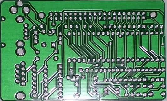
Most layout engineers treat FR4 PCB minimum trace spacing as a fixed number pulled from the fab capability table. That approach works until the first yield drop or the first hipot failure. The real constraint is never just the number printed on the quote. It is the combination of etch tolerance, copper weight, voltage stress, and how the board will actually be processed.
When clearance is pushed too hard, the usual result is not an immediate open. It is intermittent bridging that only appears after moisture absorption or thermal cycling.
What "Minimum Trace Spacing" Actually Means on FR4
On a finished FR4 board the measured space between two copper features is not the same number that was drawn in the CAD file. Etching undercuts the copper, so a 5 mil designed gap can easily become 4.2–4.5 mil on the outer layers after the process finishes. Inner layers see less undercut but still move with registration error.
The number that matters for reliability is the final copper-to-copper distance after all process tolerances, not the design value. That is why a 4 mil FR4 PCB clearance that looks fine in Gerber often fails electrical test or field hipot once the board has seen humidity.
How Voltage Forces Larger Clearance Than the Fab Can Deliver
IPC-2221 still gives the cleanest starting numbers. For external conductors at sea level the table calls for 0.1 mm (≈4 mil) up to 30 V, then steps up quickly. Between 31–50 V the requirement jumps to 0.6 mm. Above 100 V the numbers become large enough that most dense layouts simply cannot meet them without moving to higher layer counts or different stack-ups.
Many boards sit in the awkward zone: 48 V rails, 60 V motor drivers, or isolated DC-DC stages that need more than the 5–6 mil FR4 PCB minimum trace spacing the fab quotes for "standard process." Designers often keep the tight spacing and rely on soldermask or conformal coating to "make up the difference." That works only until the coating has a void or the board is used in a high-humidity environment.
Internal layers get a little more forgiveness because the dielectric is continuous, but the same voltage tables still apply. A 4 mil internal clearance that survives fabrication can still arc under 150 V if the prepreg has voids or the resin content is low.
Real Factory Limits on FR4 Trace Spacing
Standard FR4 process capability is still driven by the etching chemistry and the copper thickness. For 1 oz outer copper most shops will quote 4/4 mil or 5/5 mil as their baseline. Move to 2 oz and the minimum reliable space jumps to 6–8 mil because the longer etch time increases undercut and the risk of copper residual in the gaps.
Inner layers with 0.5 oz or 1 oz copper can go tighter, sometimes 3.5/3.5 mil, but only if the shop runs laser direct imaging and controlled impedance etching. Once the copper weight exceeds 2 oz the process window narrows fast. Residual copper between traces becomes the dominant yield killer.
Registration error adds another 1–1.5 mil of uncertainty on outer layers. That means a design that is exactly at the quoted minimum is already at risk before the board ever leaves the plating line.

Where Tight Spacing Actually Causes Failures
The most common field failure is not a hard short at ICT. It is intermittent leakage that only appears after the board has absorbed moisture and then sees voltage. FR4 is hygroscopic. A 4 mil gap that is clean when the board is dry can support enough surface leakage under 80 % RH to trip residual-current detection or slowly degrade the insulation resistance.
Assembly adds its own risks. Solder paste that smears or flux residue that is not fully cleaned will bridge gaps that were already marginal. Fine-pitch BGA escape routing is especially vulnerable because the local density forces the designer to stay at the absolute minimum FR4 PCB clearance across many nets.
Long-term reliability suffers when the board is used in outdoor or industrial environments. Thermal expansion mismatch plus repeated voltage stress across a narrow gap accelerates dendritic growth. Once a dendrite forms, the failure is permanent.
Setting Design Clearance That Survives Real Production
Start with the voltage requirement, not the fab capability table. If the working voltage is under 30 V and the board is sealed or coated, 5 mil outer / 4 mil inner is usually safe for 1 oz copper. Once voltage climbs above 50 V, open the outer-layer clearance to at least 8–10 mil even if the fab says they can do 5 mil.
For 2 oz copper, treat 8 mil as the practical floor on outer layers unless the shop has demonstrated controlled etching on that weight. Do not rely on soldermask to provide electrical isolation; soldermask is a process aid, not a dielectric barrier.
When density forces tighter spacing, move critical high-voltage nets to inner layers where the continuous dielectric gives better protection, or increase the layer count so that the high-voltage pairs can be routed with proper clearance. Adding a guard trace or increasing the local copper-to-copper distance only on the high-voltage nets is often cheaper than a full process upgrade.
Always leave a 20–25 % margin above the calculated minimum. Etch tolerance, registration, and copper thickness variation will consume that margin. If the calculated number is 5 mil, design to 6.5–7 mil. The extra space almost never costs more real estate than the scrap and field returns that come from running at the absolute limit.

Final check before release: ask the fab for their actual etch-back data on the copper weight and process you intend to use. The quoted "minimum" is a marketing number. The process capability data is the engineering number. Use the latter when you set the FR4 PCB minimum trace spacing rules in the design.