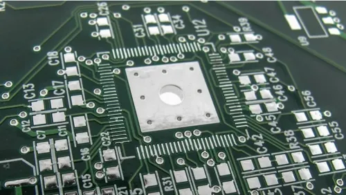
In production we handle FR4 PCB thickness selection by locking the finished board thickness to materials we already stock and process daily. CAM engineers open the stackup request and immediately check whether the target thickness can be built from standard cores and prepregs. If the design calls for 0.8 mm, 1.0 mm, 1.2 mm, 1.6 mm or 2.0 mm we build it with normal process parameters and standard press cycles. Anything outside that list forces a special material order or a non-standard prepreg combination, which we flag in DFM before the job is released to the floor.
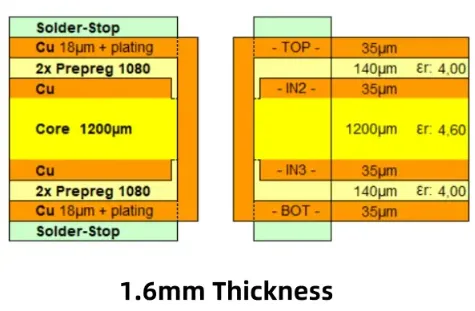
Which finished thicknesses actually sit on the material rack
Most fabrication houses keep a limited set of cores: 0.1 mm, 0.2 mm, 0.3 mm, 0.4 mm, 0.5 mm, 0.6 mm, 0.8 mm and 1.0 mm, plus the usual 1080, 2116 and 7628 prepregs. Finished board thickness is the sum of those cores, prepregs, copper foils and the plated copper added in the holes and on the outer layers. After press and plating the real finished thickness for a nominal 1.6 mm board usually lands between 1.45 mm and 1.75 mm. That is why we quote ±10 % or ±0.13 mm, whichever is tighter, for standard Class 2 work. Thinner boards such as 0.4 mm and 0.6 mm are available but only from thinner cores; the process window shrinks and the material cost rises because those cores are lower-volume stock.
When a customer asks for 1.5 mm or 1.8 mm we still try to hit it, but we have to mix non-standard core/prepreg combinations. That means the material has to be ordered, the press recipe has to be validated, and the lead time stretches by one to two weeks. From a production standpoint the common thicknesses are simply the ones that keep the line moving without special handling.
Why thickness becomes a process constraint the moment the board leaves the press
Board thickness is not just a number on the drawing. It directly controls mechanical stiffness, drill aspect ratio, plating uniformity and final assembly fit. In the press the resin flow and the copper density on each layer change the final thickness by several tens of microns. After plating the outer copper and the hole walls add more thickness, so the CAM calculation must already include an expected plating build-up of 20–30 µm per side. If that calculation is off, the board either comes out thin and flexible or thick and hard to depanel.
Drill aspect ratio is the next hard limit. For a 1.6 mm board a 0.3 mm drill gives an aspect ratio of roughly 5.3 : 1, which is comfortable. On a 2.4 mm board the same drill jumps to 8 : 1 and plating quality starts to suffer in the hole center. Thin boards under 0.8 mm bring the opposite problem: the panel flexes under the drill pressure and registration drifts, especially on large panels. Routing and scoring also change with thickness; a thin board is more likely to chip or crack at the break-away tabs, while a thick board needs more force and can leave burrs that interfere with connectors.
What shows up on the floor when thickness is left uncontrolled
If the finished thickness drifts outside the allowed window the first failures appear in mechanical handling. Thin boards warp after reflow or during shipping; the warp can exceed 0.75 % and the boards fail flatness checks at the customer. During depanel a thin board often cracks along the score line or at the mouse-bite, producing scrap that is discovered only after electrical test. Thick boards create assembly problems: edge connectors no longer seat fully, press-fit pins bottom out or the board will not slide into a card-edge slot that was designed for 1.6 mm.
Impedance also moves. Dielectric thickness is the dominant variable in controlled-impedance traces. A 0.1 mm shift in core or prepreg thickness can push a 50 Ω single-ended line outside the ±10 % tolerance band. On multilayer boards that same shift changes the overall finished thickness and can make the board too thick for the mechanical enclosure or too thin for the required stiffness under vibration. In high-volume runs these issues turn into yield loss, rework of the entire panel lot, or delayed shipment while new material is ordered.
How CAM and process control actually lock the thickness
We start with a stackup table that lists every available core and prepreg with its measured pressed thickness under our standard press cycle. CAM engineers enter the copper weights and the target finished thickness; the software calculates the combination that lands closest to the nominal value after plating. For a 1.6 mm 4-layer board the typical build is 0.2 mm core + two 2116 prepregs + outer foils, adjusted so the pressed dielectric stack plus copper equals 1.55–1.65 mm before final plating. Once the stackup is frozen we apply a process compensation of +0.02 mm to +0.04 mm to account for copper plating and surface finish.
On the floor the press recipe is fixed for each material set. We measure thickness at first-article with a calibrated micrometer at nine points across the panel. If the average is outside ±10 % we stop the lot, adjust the prepreg count or the press pressure, and re-qualify. For impedance-critical jobs we also cut a cross-section coupon and measure the actual dielectric thickness under microscope; that data feeds back into the next CAM calculation. Panel design helps as well: we keep copper distribution balanced and avoid large copper-free areas that cause resin starvation and local thickness variation.
Connector and assembly requirements are checked at the same time. If the design uses a standard card-edge connector rated for 1.6 mm, we refuse a 1.2 mm or 2.0 mm finished thickness unless the customer explicitly accepts the mechanical risk. Press-fit connectors have even tighter limits; the plated hole diameter and the board thickness must both stay inside the connector vendor's recommended window or the pins will not retain properly.
When we allow a non-standard thickness
Exceptions are accepted when the application truly needs it and the customer accepts the trade-offs. High-power boards that require extra copper and thicker dielectrics for thermal or voltage isolation, or very thin boards for space-constrained wearables, can be run. In those cases we order the special cores, validate the press and drill recipes on a small pilot lot, and quote the extra material cost plus longer lead time. Prototype quantities under 50 panels are easier to accommodate than volume production; once the job moves to thousands of panels the material and process risk become too high and we push back to a standard thickness. The decision is always documented in the DFM report so both sides know the risk that was accepted.