Multilayer PCB Grounding
Multilayer PCB grounding plays a critical role in ensuring the reliability and performance of complex electronic designs. In multilayer printed circuit boards, which often feature multiple layers of conductive traces separated by insulating materials, effective grounding strategies are essential to minimize electromagnetic interference, reduce noise, and maintain signal integrity. This tag, Multilayer PCB Grounding, encompasses a collection of articles that delve into the principles and techniques for implementing robust grounding systems in these advanced PCBs. Whether you are designing high-speed digital circuits, RF applications, or power electronics, understanding how to properly configure ground planes, vias, and return paths can prevent issues like crosstalk, ground loops, and voltage fluctuations that compromise system functionality. For engineers and hobbyists searching for guidance on this topic, the content here offers practical insights into best practices such as dedicating entire layers to ground planes, optimizing via stitching for low-impedance paths, and incorporating split grounds where necessary to isolate noisy sections. These approaches not only enhance electromagnetic compatibility but also support compliance with industry standards like IPC-2221. Real-world applications include automotive electronics, where stable grounding ensures sensor accuracy, or telecommunications devices that demand minimal signal distortion. By applying these techniques, designers can achieve better thermal management and overall board efficiency, leading to more reliable products. Browsing the articles linked under this tag provides detailed case studies, step-by-step tutorials, and troubleshooting tips tailored to common challenges in multilayer PCB design. This resource equips you with the knowledge to refine your grounding strategies and elevate your projects to professional standards.
Technical Articles
Analog-Driven SoC Design Choices in Sub-7nm Processes: Challenges & Strategies
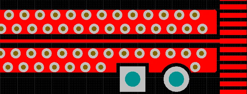
Ground Plane Stitching: Achieving Optimal Grounding in Multi Layer PCBs
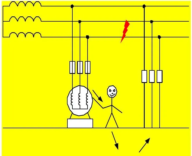
Why Grounding Resistance Is Limited to 4 Ω
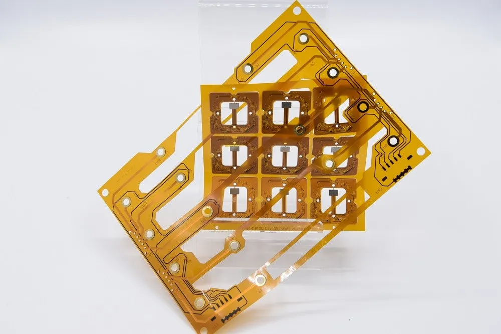
Why Large Ground Openings Can Cause Manufacturing Problems in FPC?
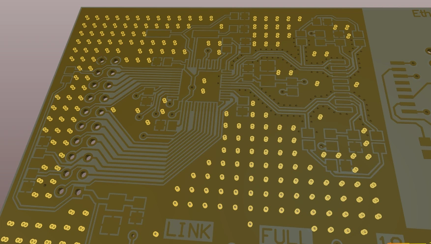
The Ultimate Guide to Via Stitching in Multi Layer PCBs: Best Practices
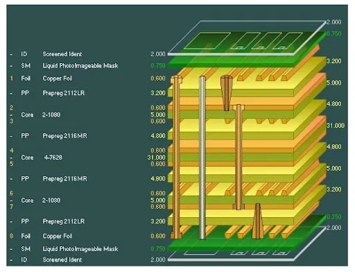
Ground and Power Structures and Routing on Multi Layer Boards
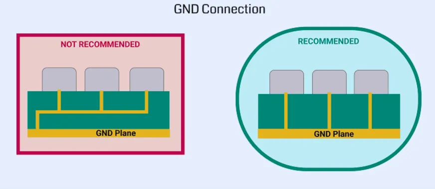
PCB Grounding Techniques: A Guide to Minimizing Noise and Ensuring Reliable Connections
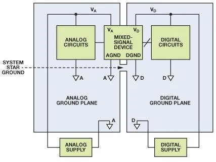
PCB Ground Plane Stack Up: Choosing the Right Configuration for Your Design

Measuring Ground Resistance with a Ground Tester
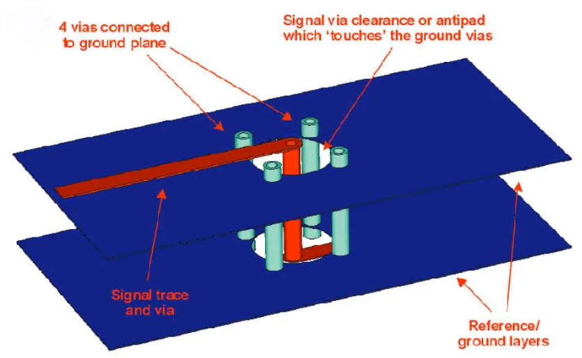
Via Stitching: A Comprehensive Guide to Enhancing Grounding and Shielding in PCBs
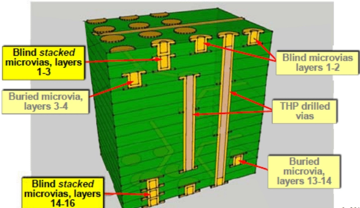
Reducing EMI in High Layer Count PCBs: Shielding and Grounding Techniques
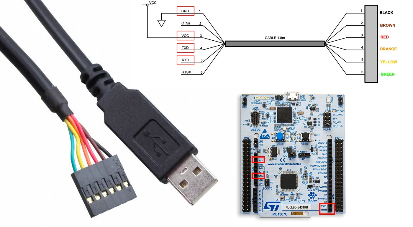
STM32 UART Communication: Principles, Implementation, and PCB Design Considerations
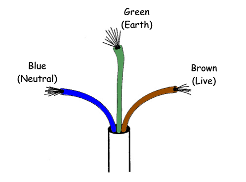
Why the Neutral Wire Can't Be Replaced by Earth
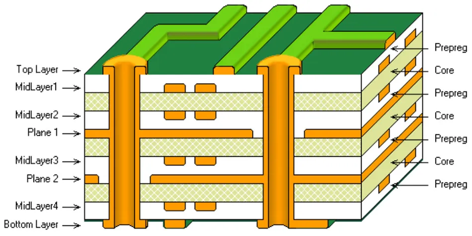
Multi-Layer PCBs: A Beginner's Guide to Design and Fabrication
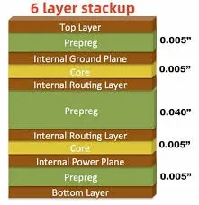
Designing a 6-Layer PCB for EMI/EMC Compliance: A Comprehensive Guide

Instrumentation Amplifiers: Principles, Derivation, and PCB Design Considerations
Get in Touch
Send Message
- Products & Service
- Company
- About AIVON
- Contact
- News
- Blog
- Certification
-


- Payment
-


2026 AIVON.COM All Rights Reserved