Introduction
Instrumentation amplifiers (In-Amps) are specialized differential amplifiers designed for precise amplification of small signals in the presence of large common-mode noise. They are fundamental building blocks in data acquisition systems, sensor interfaces, medical instrumentation, and industrial measurement equipment. For electronics engineers and PCB manufacturers, proper implementation of In-Amps demands careful attention to analog layout, component matching, grounding, and noise minimization to achieve high common-mode rejection ratio (CMRR) and overall system accuracy.
What is an Instrumentation Amplifier?
An instrumentation amplifier is an enhanced differential amplifier with integrated input buffering stages. This architecture provides very high input impedance, eliminating the need for precise source impedance matching. Key performance characteristics include:
- Very low DC offset and drift
- Low noise
- High open-loop gain
- Excellent CMRR (typically >100 dB)
- High input impedance
In-Amps are primarily used for low-frequency signals (below ~1 MHz) where they amplify small differential voltages while strongly rejecting common-mode signals, such as ground loops or electromagnetic interference picked up over long sensor cables. The classic topology uses three operational amplifiers and a network of precision resistors (0.1% tolerance or better) to achieve high CMRR.
Key Requirements for Instrumentation Amplifier Circuits
A high-performance In-Amp should satisfy the following engineering criteria:
- Accurate and Stable Gain - Precise, predictable amplification of low-level transducer signals.
- Easy Gain Adjustment - Typically set by a single external resistor (Rg).
- High Input Impedance - Prevents loading of high-impedance sensors.
- Low Output Impedance - Ensures compatibility with subsequent stages (ADCs, filters, etc.).
- High CMRR - Critical for rejecting common-mode noise in real-world environments.
- High Slew Rate - Supports undistorted output for dynamic signals.
How an Instrumentation Amplifier Works
A standard In-Amp consists of two input buffer op-amps followed by a differential output stage. The first stage provides high input impedance and initial differential gain. The gain-setting resistor (Rg) between the two buffer outputs controls the overall differential gain. The second stage is a standard differential amplifier that further amplifies the signal while rejecting common-mode voltage. This buffered architecture maintains excellent CMRR even when source impedances are mismatched.
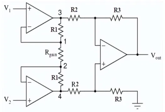
Instrumentation Amplifier Formula Derivation
The overall gain of a classic three-op-amp In-Amp is given by:
Gain = 1 + (2R / Rg)
Where R represents the matched resistors in the input stage and Rg is the external gain-setting resistor. In Stage 1 (Input Buffers), the differential voltage across Rg produces a current that is converted into amplified voltages at the buffer outputs. In Stage 2 (Differential Amplifier), this stage applies additional gain while performing common-mode rejection. The final output voltage is Vout = (V2 - V1) * Gain. Precise resistor matching in both stages is essential for maintaining high CMRR.
Common Circuit Examples
Discrete Implementation
Using components like the LM358, LM324, or LM741, designers can build In-Amps using three or four general-purpose op-amps with precision resistors. This is suitable for prototyping and cost-sensitive applications.
Integrated Solutions
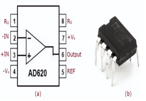
Single-chip In-Amps like the AD620 require only one external Rg. They offer superior matching, lower offset, and better CMRR in a compact footprint, making them ideal for high-precision PCB designs.
PCB Design and Electronics Manufacturing Considerations
Successful deployment of instrumentation amplifiers depends heavily on PCB layout and manufacturing quality:
- Analog Grounding and Partitioning: Use a solid ground plane with proper star grounding or analog/digital separation to minimize noise coupling.
- Component Matching and Placement: Place precision resistors close to the In-Amp package. Matched resistor networks or arrays improve CMRR and thermal tracking.
- Signal Integrity and Noise Reduction: Keep input traces short and shielded. Use guard rings around high-impedance inputs. Decoupling capacitors should be placed close to power pins.
- Thermal Management: For precision applications, minimize thermal gradients across resistors and the IC to reduce offset drift.
- Layer Stack-up: Multilayer boards with dedicated analog power and ground planes help isolate sensitive analog sections.
- Manufacturing Practices: High-reliability assembly with clean processes, controlled soldering, and post-assembly cleaning are critical. Automated optical inspection (AOI) and functional testing ensure consistent performance.
- Flexible and Rigid-Flex Solutions: Useful in compact or portable instrumentation where space is constrained.
Industry Applications and Trends
Instrumentation amplifiers are widely used in medical devices (ECG, EEG), industrial sensors, bridge amplifiers, thermocouple conditioning, and precision data acquisition systems. Modern trends include higher integration, lower power consumption, and improved rail-to-rail operation for battery-powered and IoT applications.
Supporting Precision Analog Circuits Through PCB Manufacturing
High-accuracy analog signal chains rely on expert PCB fabrication and assembly. Capabilities in controlled-impedance routing, precision component placement, low-noise design, and high-reliability processes enable OEMs to achieve the full performance potential of instrumentation amplifiers in demanding measurement and instrumentation applications.
FAQs
Q1: What is the main advantage of an instrumentation amplifier over a standard differential amplifier?
A1: Superior input impedance, easier gain setting, and significantly higher CMRR due to the buffered input stage.
Q2: How is gain typically adjusted in an In-Amp?
A2: By changing a single external resistor (Rg) connected between the input buffer stages.
Q3: Why is PCB layout critical for instrumentation amplifiers?
A3: Proper layout minimizes noise, preserves high CMRR, reduces thermal gradients, and prevents ground loops that can degrade precision in low-level signal applications.