 00:40
00:40
PCB Mass Production
PCB mass production represents a critical phase in electronics manufacturing, where designs transition from prototypes to high-volume output to meet market demands efficiently. For engineers, product developers, and manufacturers searching for insights on PCB mass production, this tag serves as a comprehensive resource, offering guidance on scaling operations while maintaining quality and cost-effectiveness. Understanding the intricacies of this process is essential for avoiding common pitfalls, such as design flaws that lead to production delays or excessive rework. Key aspects covered here include selecting reliable fabrication partners, optimizing board layouts for automated assembly, and implementing rigorous testing protocols to ensure reliability at scale. Practical applications range from consumer electronics like smartphones and wearables to industrial systems in automotive and aerospace sectors, where high yields and minimal defects are paramount. Best practices emphasize design for manufacturability (DFM) principles, such as standardizing component footprints and incorporating panelization techniques to maximize efficiency during fabrication and assembly. By focusing on these strategies, you can reduce lead times, lower per-unit costs, and enhance overall product performance. Articles under this tag delve into real-world case studies, step-by-step workflows for transitioning to mass production, and evaluations of advanced technologies like surface-mount technology (SMT) lines and automated optical inspection (AOI). Whether you are troubleshooting yield issues or exploring sustainable materials for large runs, the content provides actionable advice drawn from industry expertise. Browsing these resources can help refine your approach and stay ahead in a competitive landscape.
Video Guide
-
00:40
Technical Articles

PCB Panelization Design Optimization and Practical Considerations

Why SMT Lines Are Split into Long and Short Lines, and How to Improve SMT Production Efficiency
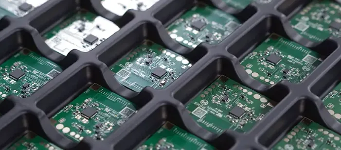
High Volume PCB Assembly: Ensuring Regulatory Compliance and Certifications
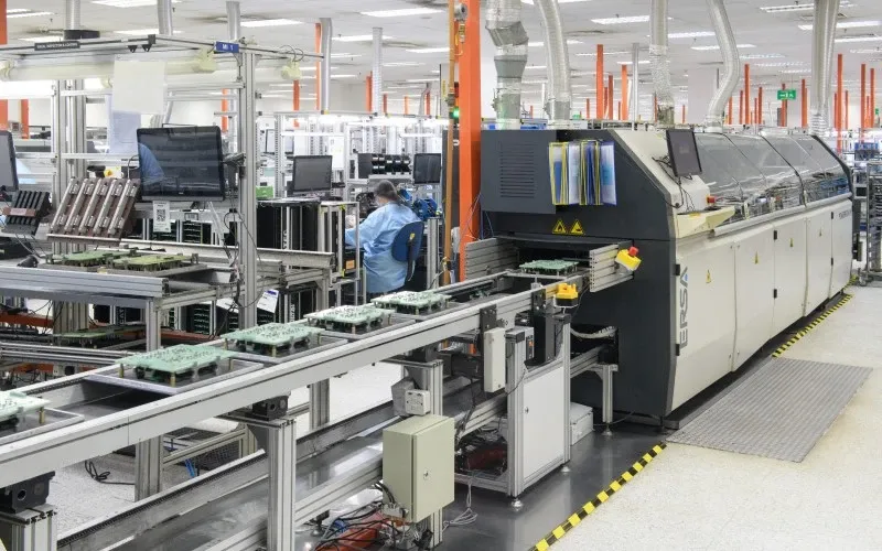
The Role of Automation in High Volume PCB Manufacturing: Improving Efficiency and Quality
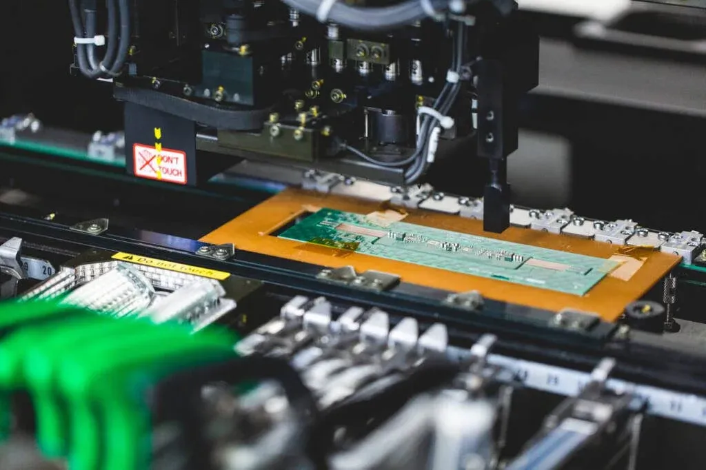
From Prototype to Production: Scaling Up Your Rigid Flex PCB Manufacturing
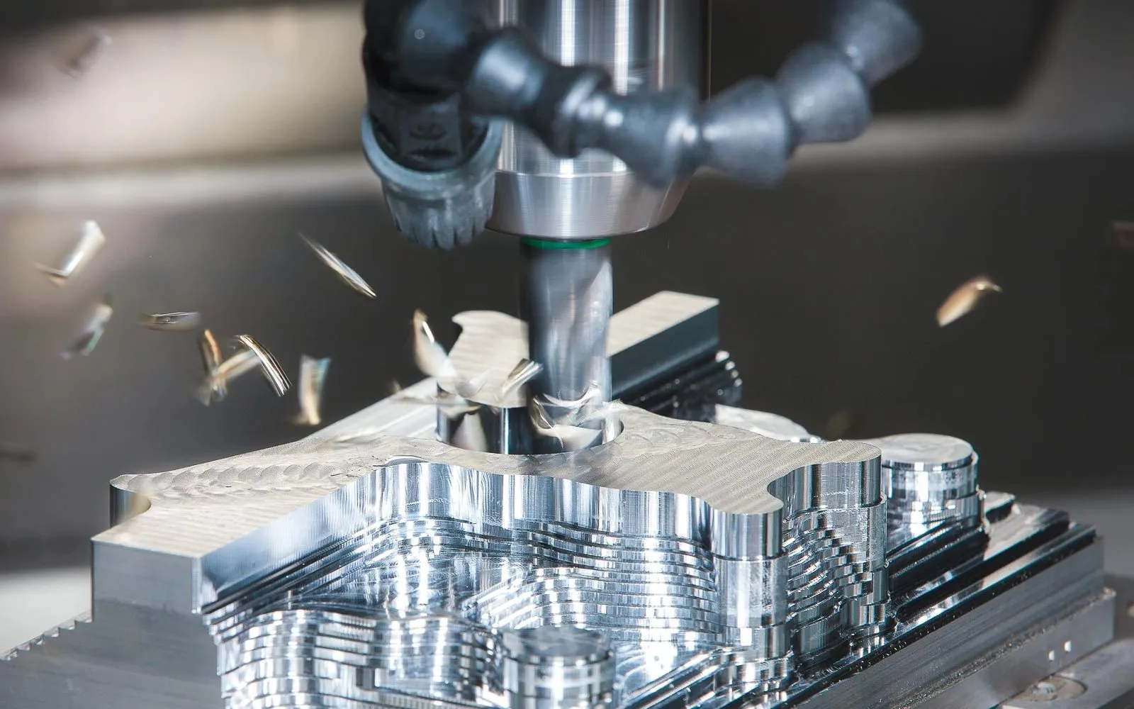
Best Materials for Prototype vs Production CNC Machining
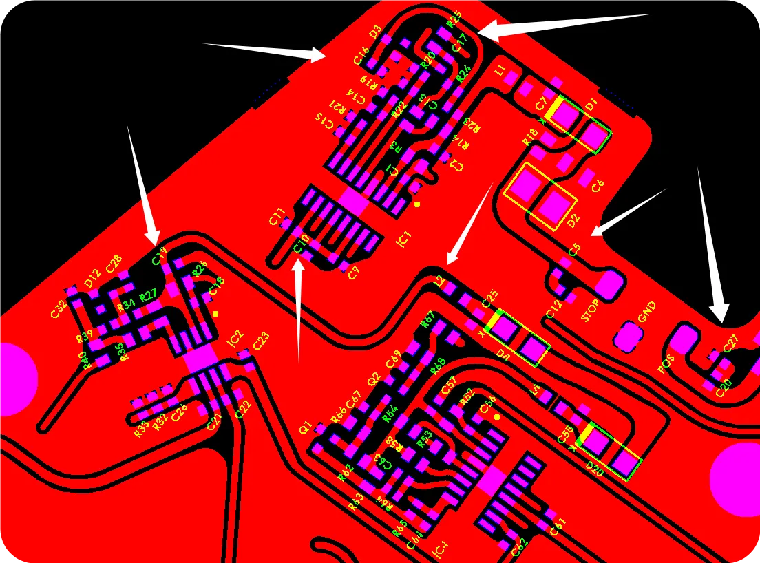
3 oz Heavy Copper PCB Production Solving Slot and V Cut Design Issues
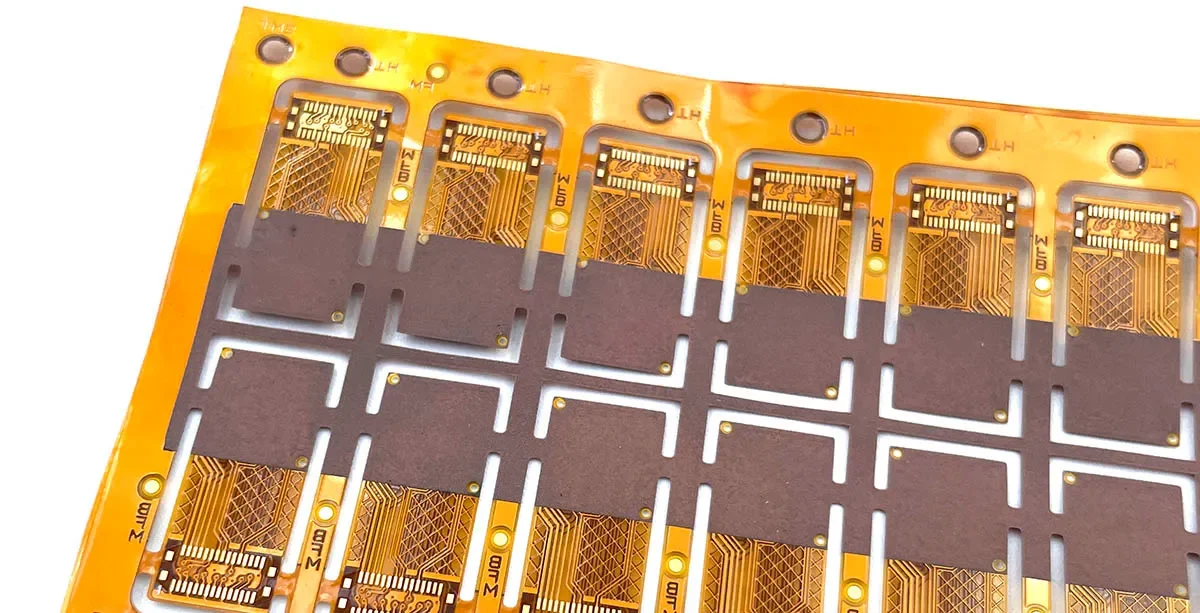
FPC Panel Size for Mass Production: What Size Works Better?

The Evolution of Mobile Operating Systems: From iOS and Android Dominance to Industry Lessons

Single 1TB Memory Module Appears Achievable

PCB Mass Production for Medical Devices: Ensuring Safety and Reliability
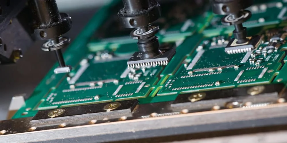
Component Placement Strategies for High Volume Assembly
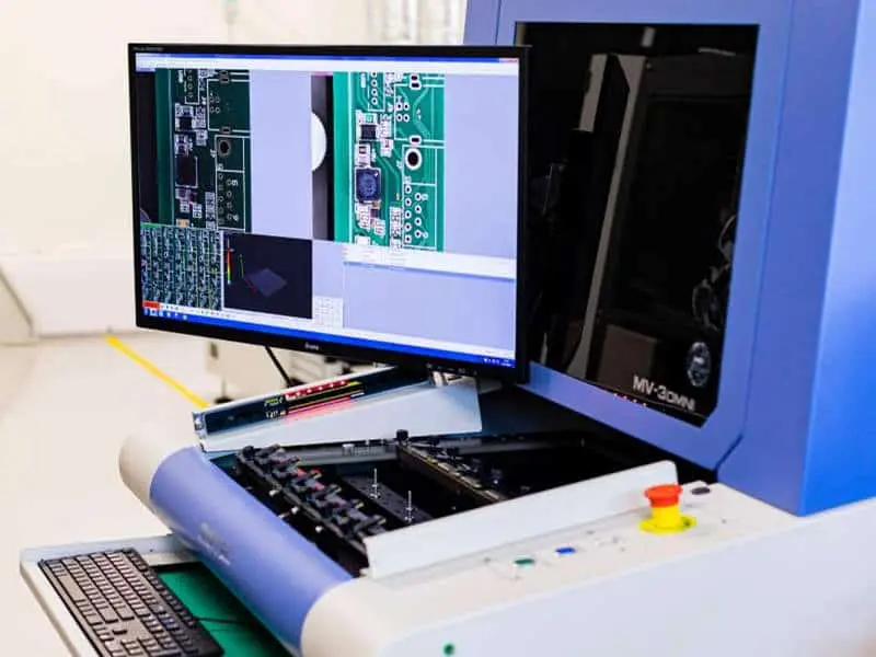
From Prototype to Production: Scaling with Quick Turn PCB Manufacturing
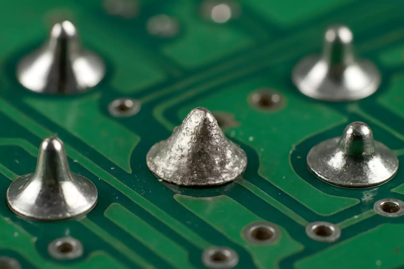
Avoiding the Pitfalls: Common Mistakes in PCB Mass Production and How to Fix Them

5G and PCB Mass Production: Designing for High-Speed Connectivity
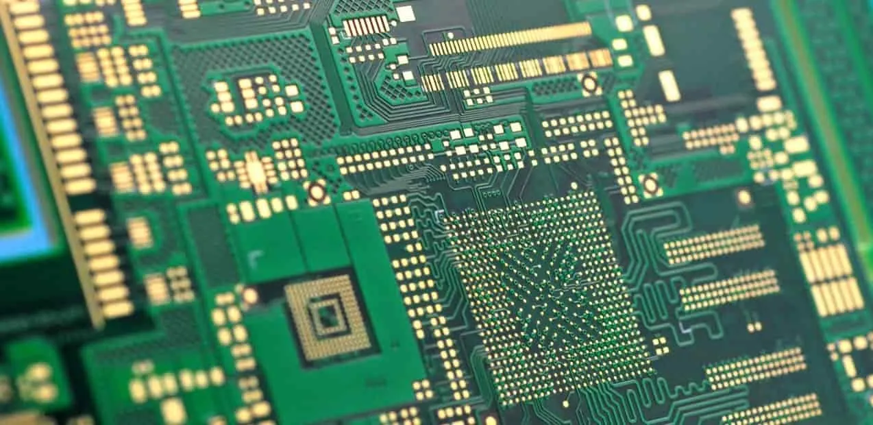
Advanced Surface Finishes: Choosing the Right Option for PCB Mass Production
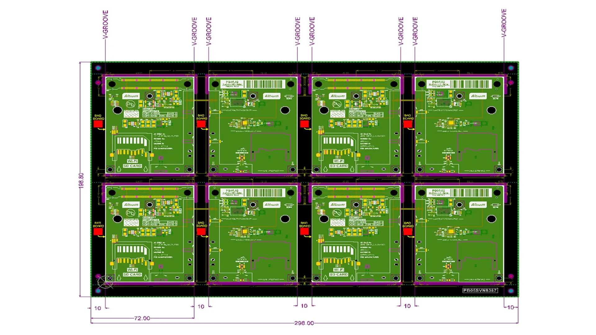
PCB Batch Production for Prototyping: Fast and Affordable
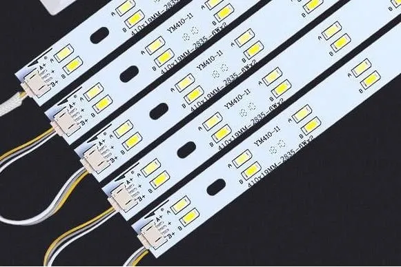
Cost-Effective Brilliance: Optimizing LED Lighting PCB Design for Mass Production

Telecommunications PCB Assembly: From Prototyping to Mass Production